DAK-89 Power Integrations, DAK-89 Datasheet - Page 13
DAK-89
Manufacturer Part Number
DAK-89
Description
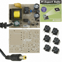
DESIGN ACCELERATOR KIT XT SWITCH
Manufacturer
Power Integrations
Series
LinkSwitch®-XTr
Specifications of DAK-89
Main Purpose
AC/DC, Primary Side
Outputs And Type
1, Isolated
Power - Output
2W
Voltage - Output
6.2V
Current - Output
322mA
Voltage - Input
85 ~ 265VAC
Regulator Topology
Flyback
Board Type
Bare (Unpopulated) and Fully Populated
Utilized Ic / Part
LNK362, LNK363, LNK364
Lead Free Status / RoHS Status
Lead free / RoHS Compliant
Frequency - Switching
-
Lead Free Status / Rohs Status
Lead free / RoHS Compliant
Other names
596-1105


8 Design Spreadsheets
Page 13 of 32
ENTER APPLICATION
VARIABLES
VACMIN
ENTER LinkSwitch-XT
VARIABLES
VACMAX
fL
VO
IO
CC Threshold
Voltage
Output Cable
Voltage Resistance
PO
Feedback Type
Add Bias Winding
Clampless design
(LNK 362 only)
n
Z
tC
CIN
Input Rectification
Type
LinkSwitch-XT
Chosen Device
ILIMITMIN
ILIMITMAX
fSmin
I^2fmin
VOR
VDS
VD
KP
ACDC_LinkSwitch
Integrations 2005
Copyright Power
-XT_101205;
Rev.1.2;
LNK362
85
265
50
6.20
0.32
0.00
Opto
No
Yes
0.63
0.50
2.90
6.60
F
77.00
0.75
INPUT
Caution
INFO
LNK362
OUTPUT
Clampless
LNK362
124000 Hertz
0.130 Amps
0.150 Amps
2199 A^2Hz
Opto
0.17
2.00
0.63
0.75 Volts
1.00
0.5
No
77 Volts
10 Volts
F
Volts
Volts
Hertz
Volts
Amps
Volts
Ohms
Watts
mSeconds
uFarads
UNIT
Tel: +1 408 414 9200 Fax: +1 408 414 9201
ACDC_LinkSwitch-XT_101205_Rev1-2.xls;
LinkSwitch-XT Continuous/Discontinuous Flyback
Transformer Design Spreadsheet
EP89
Minimum AC Input Voltage
Maximum AC Input Voltage
AC Mains Frequency
Output Voltage (main) (For CC designs enter upper
CV tolerance limit)
Power Supply Output Current (For CC designs enter
upper CC tolerance limit)
Voltage drop across sense resistor.
Enter the resistance of the output cable (if used)
Output Power (VO x IO + CC dissipation)
Enter 'BIAS' for Bias winding feedback and 'OPTO' for
Optocoupler feedback
Enter 'YES' to add a Bias winding. Enter 'NO' to
continue design without a Bias winding. Addition of
Bias winding can lower no load consumption
!!! Caution. For designs above 2 W and no Bias
winding, Verify peak Drain Voltage and EMI
performance
Efficiency Estimate at output terminals.
Loss Allocation Factor (suggest 0.5 for CC=0 V, 0.75
for CC=1 V)
Bridge Rectifier Conduction Time Estimate
Input Capacitance
Choose H for Half Wave Rectifier and F for Full Wave
Rectification
User selection for LinkSwitch-XT
Minimum Current Limit
Maximum Current Limit
Minimum Device Switching Frequency
I^2f (product of current limit squared and frequency is
trimmed for tighter tolerance)
VOR > 90V not recommended for Clampless designs
with no Bias windings. Reduce VOR below 90V
LinkSwitch-XT on-state Drain to Source Voltage
Output Winding Diode Forward Voltage Drop
Ripple to Peak Current Ratio (0.6 < KP < 6.0)
Power Integrations
www.powerint.com
Related parts for DAK-89
Image
Part Number
Description
Manufacturer
Datasheet
Request
R

Part Number:
Description:
KIT DESIGN ACCELERATOR MODEM
Manufacturer:
Power Integrations
Datasheet:

Part Number:
Description:
KIT DESIGN ACCELERATOR SET TOP
Manufacturer:
Power Integrations
Datasheet:

Part Number:
Description:
KIT REF DES DPA 6.6W DC-DC CONV
Manufacturer:
Power Integrations
Datasheet:

Part Number:
Description:
KIT DESIGN ACCELERATOR POE CONV
Manufacturer:
Power Integrations
Datasheet:

Part Number:
Description:
DESIGN ACCELERATOR KIT LP SWITCH
Manufacturer:
Power Integrations
Datasheet:

Part Number:
Description:
KIT DESIGN ACC PEAKSWITCH FAMILY
Manufacturer:
Power Integrations
Datasheet:

Part Number:
Description:
KIT DESIGN ACCELERATOR ADAPTER
Manufacturer:
Power Integrations
Datasheet:

Part Number:
Description:
KIT DESIGN ACCELERATOR ADAPTER
Manufacturer:
Power Integrations
Datasheet:

Part Number:
Description:
KIT DESIGN ACCELERATOR DC-DC
Manufacturer:
Power Integrations
Datasheet:

Part Number:
Description:
KIT DESIGN ACCELERATOR DPA SW
Manufacturer:
Power Integrations
Datasheet: