DAK-89 Power Integrations, DAK-89 Datasheet - Page 15
DAK-89
Manufacturer Part Number
DAK-89
Description
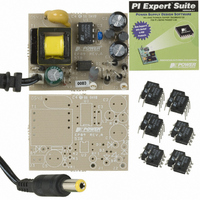
DESIGN ACCELERATOR KIT XT SWITCH
Manufacturer
Power Integrations
Series
LinkSwitch®-XTr
Specifications of DAK-89
Main Purpose
AC/DC, Primary Side
Outputs And Type
1, Isolated
Power - Output
2W
Voltage - Output
6.2V
Current - Output
322mA
Voltage - Input
85 ~ 265VAC
Regulator Topology
Flyback
Board Type
Bare (Unpopulated) and Fully Populated
Utilized Ic / Part
LNK362, LNK363, LNK364
Lead Free Status / RoHS Status
Lead free / RoHS Compliant
Frequency - Switching
-
Lead Free Status / Rohs Status
Lead free / RoHS Compliant
Other names
596-1105


Page 15 of 32
TRANSFORMER SECONDARY DESIGN
PARAMETERS
VOLTAGE STRESS
PARAMETERS
FEEDBACK
COMPONENTS
TRANSFORMER SECONDARY DESIGN
PARAMETERS (MULTIPLE OUTPUTS)
Lumped parameters
ISP
ISRMS
IRIPPLE
CMS
AWGS
DIAS
ODS
INSS
VDRAIN
PIVS
Recommended
Bias Diode
R1
R2
1st output
VO1
IO1
PO1
VD1
NS1
ISRMS1
IRIPPLE1
PIVS1
Recommended
Diodes
Pre-Load
Resistor
CMS1
AWGS1
DIAS1
ODS1
200 - 820 ohms
1N4003 -
UF4001,
1N4007
SB150
126.56 Cmils
13.00
40.03 Volts
29.00 AWG
500 -
1000
1.44 Amps
0.63 Amps
0.54 Amps
0.29 mm
0.66 mm
0.19 mm
6.20 Volts
0.32 Amps
2.00 Watts
0.75 Volts
0.63 Amps
0.54 Amps
0.29 mm
0.66 mm
125 Cmils
29 AWG
40 Volts
2 k-Ohms
- Volts
ohms
Peak Secondary Current
Secondary RMS Current
Output Capacitor RMS Ripple Current
Secondary Bare Conductor minimum circular mils
Secondary Wire Gauge (Rounded up to next larger standard
AWG value)
Secondary Minimum Bare Conductor Diameter
Secondary Maximum Outside Diameter for Triple Insulated
Wire
Maximum Secondary Insulation Wall Thickness
For Clampless designs, the Peak Drain Voltage is highly
dependent on Transformer capacitance and leakage
inductance. Please verify this on the bench and ensure that it
is below 650 V to allow 50 V margin for transformer variation.
Output Rectifier Maximum Peak Inverse Voltage
Recommended diode is 1N4003. Place diode on return leg of
bias winding for optimal EMI. See LinkSwitch-XT Design
Guide
CV bias resistor for CV/CC circuit. See LinkSwitch-XT Design
Guide
Resistor to set CC linearity for CV/CC circuit. See LinkSwitch-
XT Design Guide
Main Output Voltage (if unused, defaults to single output
design)
Output DC Current
Output Power
Output Diode Forward Voltage Drop
Output Winding Number of Turns
Output Winding RMS Current
Output Capacitor RMS Ripple Current
Output Rectifier Maximum Peak Inverse Voltage
Recommended Diodes for this output
Recommended value of pre-load resistor
Output Winding Bare Conductor minimum circular mils
Wire Gauge (Rounded up to next larger standard AWG
value)
Minimum Bare Conductor Diameter
Maximum Outside Diameter for Triple Insulated Wire
Tel: +1 408 414 9200 Fax: +1 408 414 9201
Power Integrations
www.powerint.com
Related parts for DAK-89
Image
Part Number
Description
Manufacturer
Datasheet
Request
R

Part Number:
Description:
KIT DESIGN ACCELERATOR MODEM
Manufacturer:
Power Integrations
Datasheet:

Part Number:
Description:
KIT DESIGN ACCELERATOR SET TOP
Manufacturer:
Power Integrations
Datasheet:

Part Number:
Description:
KIT REF DES DPA 6.6W DC-DC CONV
Manufacturer:
Power Integrations
Datasheet:

Part Number:
Description:
KIT DESIGN ACCELERATOR POE CONV
Manufacturer:
Power Integrations
Datasheet:

Part Number:
Description:
DESIGN ACCELERATOR KIT LP SWITCH
Manufacturer:
Power Integrations
Datasheet:

Part Number:
Description:
KIT DESIGN ACC PEAKSWITCH FAMILY
Manufacturer:
Power Integrations
Datasheet:

Part Number:
Description:
KIT DESIGN ACCELERATOR ADAPTER
Manufacturer:
Power Integrations
Datasheet:

Part Number:
Description:
KIT DESIGN ACCELERATOR ADAPTER
Manufacturer:
Power Integrations
Datasheet:

Part Number:
Description:
KIT DESIGN ACCELERATOR DC-DC
Manufacturer:
Power Integrations
Datasheet:

Part Number:
Description:
KIT DESIGN ACCELERATOR DPA SW
Manufacturer:
Power Integrations
Datasheet: