DAK-89 Power Integrations, DAK-89 Datasheet - Page 14
DAK-89
Manufacturer Part Number
DAK-89
Description
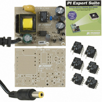
DESIGN ACCELERATOR KIT XT SWITCH
Manufacturer
Power Integrations
Series
LinkSwitch®-XTr
Specifications of DAK-89
Main Purpose
AC/DC, Primary Side
Outputs And Type
1, Isolated
Power - Output
2W
Voltage - Output
6.2V
Current - Output
322mA
Voltage - Input
85 ~ 265VAC
Regulator Topology
Flyback
Board Type
Bare (Unpopulated) and Fully Populated
Utilized Ic / Part
LNK362, LNK363, LNK364
Lead Free Status / RoHS Status
Lead free / RoHS Compliant
Frequency - Switching
-
Lead Free Status / Rohs Status
Lead free / RoHS Compliant
Other names
596-1105


Rev. E 11/08
2-14
14
.240 (6.10)
.260 (6.60)
14
.100 (2.54) BSC
.125 (3.18)
.145 (3.68)
-T-
.032 (.81)
.037 (.94)
Pin 1
.125 (3.18)
.145 (3.68)
-E-
.240 (6.10)
.260 (6.60)
-D-
SEATING
PLANE
Pin 1
-E-
-D-
LNK362-364
.014 (.36)
.022 (.56)
⊕
.367 (9.32)
.387 (9.83)
⊕
D S .004 (.10)
D S .004 (.10)
.100 (2.54) (BSC)
.367 (9.32)
.387 (9.83)
.048 (1.22)
.053 (1.35)
⊕
T E D S .010 (.25) M
.048 (1.22)
.053 (1.35)
.137 (3.48)
.009 (.23)
MINIMUM
.137 (3.48)
⊕
MINIMUM
.372 (9.45)
.388 (9.86)
E S
.057 (1.45)
.068 (1.73)
.120 (3.05)
.140 (3.56)
.057 (1.45)
.068 (1.73)
MINIMUM
(NOTE 6)
.015 (.38)
(NOTE 5)
.010 (.25)
SMD-8B
DIP-8B
.004 (.10)
.012 (.30)
Notes:
1. Package dimensions conform to JEDEC specification
2. Controlling dimensions are inches. Millimeter sizes are
3. Dimensions shown do not include mold flash or other
4. Pin locations start with Pin 1, and continue counter-clock-
5. Minimum metal to metal spacing at the package body for
6. Lead width measured at package body.
7. Lead spacing measured with the leads constrained to be
Pin 1
MS-001-AB (Issue B 7/85) for standard dual-in-line (DIP)
package with .300 inch row spacing.
shown in parentheses.
protrusions. Mold flash or protrusions shall not exceed
.006 (.15) on any side.
wise to Pin 8 when viewed from the top. The notch and/or
dimple are aids in locating Pin 1. Pin 6 is omitted.
the omitted lead location is .137 inch (3.48 mm).
perpendicular to plane T.
Solder Pad Dimensions
.004 (.10)
.046 .060
.008 (.20)
.015 (.38)
.086
.300 (7.62) BSC
.186
.036 (0.91)
.044 (1.12)
.300 (7.62)
.390 (9.91)
(NOTE 7)
.286
.060 .046
.080
.420
0 -
°
8
Notes:
1. Controlling dimensions are
2. Dimensions shown do not
3. Pin locations start with Pin 1,
4. Minimum metal to metal
5. Lead width measured at
6. D and E are referenced
°
inches. Millimeter sizes are
shown in parentheses.
include mold flash or other
protrusions. Mold flash or
protrusions shall not exceed
.006 (.15) on any side.
and continue counter-clock-
wise to Pin 8 when viewed
from the top. Pin 6 is omitted.
spacing at the package body
for the omitted lead location
is .137 inch (3.48 mm).
package body.
datums on the package
body.
PI-2551-121504
PI-2546-121504
G08B
P08B
Related parts for DAK-89
Image
Part Number
Description
Manufacturer
Datasheet
Request
R

Part Number:
Description:
KIT DESIGN ACCELERATOR MODEM
Manufacturer:
Power Integrations
Datasheet:

Part Number:
Description:
KIT DESIGN ACCELERATOR SET TOP
Manufacturer:
Power Integrations
Datasheet:

Part Number:
Description:
KIT REF DES DPA 6.6W DC-DC CONV
Manufacturer:
Power Integrations
Datasheet:

Part Number:
Description:
KIT DESIGN ACCELERATOR POE CONV
Manufacturer:
Power Integrations
Datasheet:

Part Number:
Description:
DESIGN ACCELERATOR KIT LP SWITCH
Manufacturer:
Power Integrations
Datasheet:

Part Number:
Description:
KIT DESIGN ACC PEAKSWITCH FAMILY
Manufacturer:
Power Integrations
Datasheet:

Part Number:
Description:
KIT DESIGN ACCELERATOR ADAPTER
Manufacturer:
Power Integrations
Datasheet:

Part Number:
Description:
KIT DESIGN ACCELERATOR ADAPTER
Manufacturer:
Power Integrations
Datasheet:

Part Number:
Description:
KIT DESIGN ACCELERATOR DC-DC
Manufacturer:
Power Integrations
Datasheet:

Part Number:
Description:
KIT DESIGN ACCELERATOR DPA SW
Manufacturer:
Power Integrations
Datasheet: