DAK-89 Power Integrations, DAK-89 Datasheet - Page 6
DAK-89
Manufacturer Part Number
DAK-89
Description
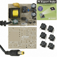
DESIGN ACCELERATOR KIT XT SWITCH
Manufacturer
Power Integrations
Series
LinkSwitch®-XTr
Specifications of DAK-89
Main Purpose
AC/DC, Primary Side
Outputs And Type
1, Isolated
Power - Output
2W
Voltage - Output
6.2V
Current - Output
322mA
Voltage - Input
85 ~ 265VAC
Regulator Topology
Flyback
Board Type
Bare (Unpopulated) and Fully Populated
Utilized Ic / Part
LNK362, LNK363, LNK364
Lead Free Status / RoHS Status
Lead free / RoHS Compliant
Frequency - Switching
-
Lead Free Status / Rohs Status
Lead free / RoHS Compliant
Other names
596-1105


Figure 6. Recommended Printed Circuit Layout for LinkSwitch-XT using P Package in a Flyback Converter Confi guration.
Bypass Capacitor C
The BYPASS pin capacitor should be located as near as possible
to the BYPASS and SOURCE pins.
Primary Loop Area
The area of the primary loop that connects the input fi lter
capacitor, transformer primary and LinkSwitch-XT together
should be kept as small as possible.
Primary Clamp Circuit
A clamp is used to limit peak voltage on the DRAIN pin at
turn-off. This can be achieved by using an RCD clamp or a
Zener (~200 V) and diode clamp across the primary winding.
In all cases, to minimize EMI, care should be taken to minimize
the circuit path from the clamp components to the transformer
and LinkSwitch-XT.
Thermal Considerations
The copper area underneath the LinkSwitch-XT acts not only
as a single point ground, but also as a heatsink. As this area is
connected to the quiet source node, it should be maximized for
Rev. E 11/08
2-6
6
6
OUT
DC
+
-
TOP VIEW
LNK362-364
BP
m
T
a
n
s
o
e
r
r
r
f
Capacitor
Y1-
Output Filter
Capacitor
D
S
S
coupler
Opto-
good heat sinking of LinkSwitch-XT. The same applies to the
cathode of the output diode.
Y-Capacitor
The placement of the Y-type cap should be directly from the
primary input fi lter capacitor positive terminal to the common/
return terminal of the transformer secondary. Such a placement
will route high magnitude common-mode surge currents away
from the LinkSwitch-XT device. Note that if an input pi (C, L, C)
EMI fi lter is used, then the inductor in the fi lter should be placed
between the negative terminals of the input fi lter capacitors.
Optocoupler
Place the optocoupler physically close to the LinkSwitch-XT to
minimize the primary-side trace lengths. Keep the high current,
high-voltage drain and clamp traces away from the optocoupler
to prevent noise pick up.
Output Diode
For best performance, the area of the loop connecting the
secondary winding, the output diode and the output fi lter
S
S
S
Maximize hatched copper
areas (
heatsinking
BP
S
FB
C
BP
) for optimum
-
HV DC
INPUT
+
PI-4155-102705
Input Filter
Capacitor
Related parts for DAK-89
Image
Part Number
Description
Manufacturer
Datasheet
Request
R

Part Number:
Description:
KIT DESIGN ACCELERATOR MODEM
Manufacturer:
Power Integrations
Datasheet:

Part Number:
Description:
KIT DESIGN ACCELERATOR SET TOP
Manufacturer:
Power Integrations
Datasheet:

Part Number:
Description:
KIT REF DES DPA 6.6W DC-DC CONV
Manufacturer:
Power Integrations
Datasheet:

Part Number:
Description:
KIT DESIGN ACCELERATOR POE CONV
Manufacturer:
Power Integrations
Datasheet:

Part Number:
Description:
DESIGN ACCELERATOR KIT LP SWITCH
Manufacturer:
Power Integrations
Datasheet:

Part Number:
Description:
KIT DESIGN ACC PEAKSWITCH FAMILY
Manufacturer:
Power Integrations
Datasheet:

Part Number:
Description:
KIT DESIGN ACCELERATOR ADAPTER
Manufacturer:
Power Integrations
Datasheet:

Part Number:
Description:
KIT DESIGN ACCELERATOR ADAPTER
Manufacturer:
Power Integrations
Datasheet:

Part Number:
Description:
KIT DESIGN ACCELERATOR DC-DC
Manufacturer:
Power Integrations
Datasheet:

Part Number:
Description:
KIT DESIGN ACCELERATOR DPA SW
Manufacturer:
Power Integrations
Datasheet: