RDK-91 Power Integrations, RDK-91 Datasheet - Page 12
RDK-91
Manufacturer Part Number
RDK-91
Description
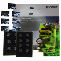
KIT DESIGN REF TINYSWITCH-III
Manufacturer
Power Integrations
Series
TinySwitch®-IIIr
Specifications of RDK-91
Main Purpose
AC/DC, Primary Side
Outputs And Type
1, Non-Isolated
Power - Output
12W
Voltage - Output
12V
Current - Output
1A
Voltage - Input
85 ~ 265VAC
Regulator Topology
Flyback
Board Type
Fully Populated
Utilized Ic / Part
TNY274, TNY275, TNY276, TNY277, TNY278, TNY279, TNY280
Product
Accessories & Kits
Lead Free Status / RoHS Status
Lead free / RoHS Compliant
Frequency - Switching
-
Other names
596-1194


Rev. I 01/09
Absolute Maximum Ratings
DRAIN Voltage .............................................................................. -0.3 V to 700 V
DRAIN Peak Current:
EN/UV Voltage ................................................................................... -0.3 V to 9 V
EN/UV Current ........................................................... .................................. 100 mA
BP/M Voltage .................................................. ....................................-0.3 V to 9 V
Storage Temperature .............................................................-65 °C to 150 °C
Operating Junction Temperature
Thermal Impedance
Thermal Impedance: P or G Package:
Output Frequency
in Standard Mode
Maximum Duty Cycle
EN/UV Pin Upper
Turnoff Threshold
Current
EN/UV Pin
Voltage
DRAIN Supply Current
Control Functions
12
Parameter
TNY274-280
(θ
(θ
JA
JC
) ............................ .................... 70 °C/W
)
(1)
TNY274 ....................................... 400 (750) mA
TNY275 .....................................560 (1050) mA
TNY276 ..................................... 720 (1350) mA
TNY277 .....................................880 (1650) mA
TNY278 .................................. 1040 (1950) mA
TNY279 ................................. 1200 (2250) mA
TNY280 ................................ 1360 (2550) mA
............................................... ............................11 °C/W
Symbol
DC
(1,4)
f
V
(3)
I
OSC
I
I
DIS
S1
S2
EN
MAX
............................... -40 °C to 150 °C
See Figure 4
Switching at f
T
SOURCE = 0 V; T
J
EN/UV Open
EN/UV Current > I
See Note B
= 25 °C
(MOSFET
(Unless Otherwise Specifi ed)
Switching) See Note A
(2)
; 60 °C/W
See Figure 16
I
I
EN/UV
Conditions
OSC
EN/UV
S1 Open
)
= -25 μA
= 25 μA
Peak-to-peak Jitter
(2)
(2)
(2)
(2)
(2)
(2)
(2)
J
(3)
DIS
= -40 to 125 °C
(MOSFET Not
Lead Temperature
Notes:
1. All voltages referenced to SOURCE, T
2. The higher peak DRAIN current is allowed while the DRAIN
3. Normally limited by internal circuitry.
4. 1/16 in. from case for 5 seconds.
5. Maximum ratings specifi ed may be applied one at a time,
Notes:
1. Measured on the SOURCE pin close to plastic interface.
2. Soldered to 0.36 sq. in. (232 mm
3. Soldered to 1 sq. in. (645 mm
Average
voltage is simultaneously less than 400 V.
without causing permanent damage to the product. Exposure
to Absolute Rating conditions for extended periods of time may
affect product reliability.
TNY274
TNY275
TNY276
TNY277
TNY278
TNY279
TNY280
(4)
.....................................................................................260 °C
-150
Min
124
1.8
0.8
62
2
), 2 oz. (610 g/m
-115
Typ
132
290
275
295
310
365
445
510
630
2
2.2
1.2
65
), 2 oz. (610 g/m
8
A
= 25 °C.
Max
140
360
400
430
460
540
640
760
-90
2.6
1.6
www.powerint.com
2
2
) copper clad.
) copper clad.
Units
kHz
μA
μA
μA
%
V
Related parts for RDK-91
Image
Part Number
Description
Manufacturer
Datasheet
Request
R

Part Number:
Description:
KIT REF DESIGN 36-72W MOTOR DRVR
Manufacturer:
Power Integrations
Datasheet:

Part Number:
Description:
KIT REF DESIGN FOR LNK457D
Manufacturer:
Power Integrations
Datasheet:

Part Number:
Description:
REFERENCE DESIGN LINKSWITCH-PH
Manufacturer:
Power Integrations
Datasheet:

Part Number:
Description:
Specifications: Manufacturer: Power Integrations ; Output Voltage: 380 VDC ; Input / Supply Voltage (Max): 264 VAC ; Input / Supply Voltage (Min): 90 VAC ; Mounting Style: Through Hole ; Output Current: 0.913 A ; Output Power: 347 W
Manufacturer:
Power Integrations, Inc.

Part Number:
Description:
KIT REF DESIGN TOP HX FOR TOP258
Manufacturer:
Power Integrations
Datasheet:

Part Number:
Description:
Power Management Modules & Development Tools TOPSwitch-JX REF. DESIGN KIT
Manufacturer:
Power Integrations
Datasheet:
Part Number:
Description:
Power Management IC Development Tools REF DESIGN RDR-292 PFF LED STREET LIGHT
Manufacturer:
Power Integrations

Part Number:
Description:
KIT REF DESIGN FOR LNK403EG
Manufacturer:
Power Integrations
Datasheet:

Part Number:
Description:
KIT REF DESIGN FOR LNK406EG
Manufacturer:
Power Integrations
Datasheet:

Part Number:
Description:
KIT REF DESIGN DG CAPZERO
Manufacturer:
Power Integrations
Datasheet:

Part Number:
Description:
KIT REF DESIGN LINKSWITCH-CV
Manufacturer:
Power Integrations
Datasheet:

Part Number:
Description:
KIT REF DESIGN LINKSWITCH 2
Manufacturer:
Power Integrations
Datasheet:

Part Number:
Description:
KIT REF DESIGN PFS762HG
Manufacturer:
Power Integrations
Datasheet:
Part Number:
Description:
Specifications: Family: Eval Boards - DC/DC & AC/DC (Off-Line) SMPS ; Series: HiperLCS™ ; Main Purpose: DC/DC, Step Down ; Outputs and Type: 1, Isolated ; Power - Output: 150W ; Voltage - Output: 24V ; Current - Output: 6.25A ; Voltage - Input:
Manufacturer:
Power Integrations, Inc.
Datasheet:

Part Number:
Description:
KIT REF DESIGN 1.2W PS TN FAMILY
Manufacturer:
Power Integrations
Datasheet: