RDK-91 Power Integrations, RDK-91 Datasheet - Page 17
RDK-91
Manufacturer Part Number
RDK-91
Description
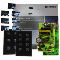
KIT DESIGN REF TINYSWITCH-III
Manufacturer
Power Integrations
Series
TinySwitch®-IIIr
Specifications of RDK-91
Main Purpose
AC/DC, Primary Side
Outputs And Type
1, Non-Isolated
Power - Output
12W
Voltage - Output
12V
Current - Output
1A
Voltage - Input
85 ~ 265VAC
Regulator Topology
Flyback
Board Type
Fully Populated
Utilized Ic / Part
TNY274, TNY275, TNY276, TNY277, TNY278, TNY279, TNY280
Product
Accessories & Kits
Lead Free Status / RoHS Status
Lead free / RoHS Compliant
Frequency - Switching
-
Other names
596-1194


NOTES:
A.
B.
C.
D.
E.
F.
G.
H.
I.
J.
K.
www.powerint.com
Nominal BP/M
Pin Cap Value
I
conditions. Total device consumption at no-load is the sum of I
Since the output MOSFET is switching, it is diffi cult to isolate the switching current from the supply current at the DRAIN. An
alternative is to measure the BP/M pin current at 6.1 V.
BP/M pin is not intended for sourcing supply current to external circuitry.
To ensure correct current limit it is recommended that nominal 0.1 μF / 1 μF / 10 μF capacitors are used. In addition, the BP/M
capacitor value tolerance should be equal or better than indicated below across the ambient temperature range of the target
application. The minimum and maximum capacitor values are guaranteed by characterization.
For current limit at other di/dt values, refer to Figure 23.
TNY274 does not set an increased current limit value, but with a 10 μF BP/M pin capacitor the current limit is the same as with a
1 μF BP/M pin capacitor (reduced current limit value).
This parameter is derived from characterization.
This parameter is derived from the change in current limit measured at 1X and 4X of the di/dt shown in the I
I
typical specifi cation under worst case application conditions (rectifi ed 265 VAC) for no-load consumption calculations.
Breakdown voltage may be checked against minimum BV
exceeding minimum BV
Auto-restart on time has the same temperature characteristics as the oscillator (inversely proportional to frequency).
S1
DSS1
0.1 μF
10 μF
1 μF
is an accurate estimate of device controller current consumption at no-load, since operating frequency is so low under these
is the worst case OFF state leakage specifi cation at 80% of BV
Tolerance Relative to Nominal
-60%
-50%
-50%
Min
DSS
.
Capacitor Value
+100%
+100%
Max
NA
DSS
specifi cation by ramping the DRAIN pin voltage up to but not
S1
and I
DSS
DSS2
and maximum operating junction temperature. I
.
TNY274-280
LIMIT
specifi cation.
DSS2
Rev. I 01/09
is a
17
Related parts for RDK-91
Image
Part Number
Description
Manufacturer
Datasheet
Request
R

Part Number:
Description:
KIT REF DESIGN 36-72W MOTOR DRVR
Manufacturer:
Power Integrations
Datasheet:

Part Number:
Description:
KIT REF DESIGN FOR LNK457D
Manufacturer:
Power Integrations
Datasheet:

Part Number:
Description:
REFERENCE DESIGN LINKSWITCH-PH
Manufacturer:
Power Integrations
Datasheet:

Part Number:
Description:
Specifications: Manufacturer: Power Integrations ; Output Voltage: 380 VDC ; Input / Supply Voltage (Max): 264 VAC ; Input / Supply Voltage (Min): 90 VAC ; Mounting Style: Through Hole ; Output Current: 0.913 A ; Output Power: 347 W
Manufacturer:
Power Integrations, Inc.

Part Number:
Description:
KIT REF DESIGN TOP HX FOR TOP258
Manufacturer:
Power Integrations
Datasheet:

Part Number:
Description:
Power Management Modules & Development Tools TOPSwitch-JX REF. DESIGN KIT
Manufacturer:
Power Integrations
Datasheet:
Part Number:
Description:
Power Management IC Development Tools REF DESIGN RDR-292 PFF LED STREET LIGHT
Manufacturer:
Power Integrations

Part Number:
Description:
KIT REF DESIGN FOR LNK403EG
Manufacturer:
Power Integrations
Datasheet:

Part Number:
Description:
KIT REF DESIGN FOR LNK406EG
Manufacturer:
Power Integrations
Datasheet:

Part Number:
Description:
KIT REF DESIGN DG CAPZERO
Manufacturer:
Power Integrations
Datasheet:

Part Number:
Description:
KIT REF DESIGN LINKSWITCH-CV
Manufacturer:
Power Integrations
Datasheet:

Part Number:
Description:
KIT REF DESIGN LINKSWITCH 2
Manufacturer:
Power Integrations
Datasheet:

Part Number:
Description:
KIT REF DESIGN PFS762HG
Manufacturer:
Power Integrations
Datasheet:
Part Number:
Description:
Specifications: Family: Eval Boards - DC/DC & AC/DC (Off-Line) SMPS ; Series: HiperLCS™ ; Main Purpose: DC/DC, Step Down ; Outputs and Type: 1, Isolated ; Power - Output: 150W ; Voltage - Output: 24V ; Current - Output: 6.25A ; Voltage - Input:
Manufacturer:
Power Integrations, Inc.
Datasheet:

Part Number:
Description:
KIT REF DESIGN 1.2W PS TN FAMILY
Manufacturer:
Power Integrations
Datasheet: