EVL6566B-65W-QR STMicroelectronics, EVL6566B-65W-QR Datasheet
EVL6566B-65W-QR
Specifications of EVL6566B-65W-QR


Related parts for EVL6566B-65W-QR


EVL6566B-65W-QR Summary of contents
Page 1
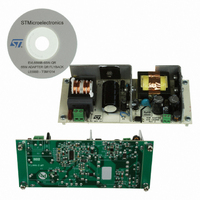
... These advantages, coupled with minimal part count required and low-cost approach of the global solution, make it a very interesting solution for powering digital consumer equipment, capable of meeting worldwide standby rules. Figure 1. EVL6566B-40WSTB demonstration board June 2010 Application note Doc ID 14630 Rev 2 ...
Page 2
Contents Contents 1 Main characteristics . . . . . . . . . . . . . . . . . . . . . . . . . . . . . . . . . . . ...
Page 3
... EVL6566B-40WSTB wakeup time at 115 Vac . . . . . . . . . . . . . . . . . . . . . . . . . . . . . . . . . . 16 Figure 13. EVL6566B-40WSTB wakeup time at 230 Vac . . . . . . . . . . . . . . . . . . . . . . . . . . . . . . . . . . 16 Figure 14. EVL6566B-40WSTB startup at 90 Vac - full load . . . . . . . . . . . . . . . . . . . . . . . . . . . . . . . . 17 Figure 15. EVL6566B-40WSTB startup at 265 Vac - full load . . . . . . . . . . . . . . . . . . . . . . . . . . . . . . . 17 Figure 16. EVL6566B-40WSTB hold-up time at 115 Vac - full load . . . . . . . . . . . . . . . . . . . . . . . . . . 18 Figure 17. EVL6566B-40WSTB hold-up time at 230 Vac - full load . . . . . . . . . . . . . . . . . . . . . . . . . . 18 Figure 18. ...
Page 4
Main characteristics 1 Main characteristics The main characteristics of this SMPS are listed below: ● Input voltage: Vin 264 Vrms f: 45-66 Hz ● Output voltages as given in Table 1. Output voltages Vout Iout 1.8 V 1.73 ...
Page 5
AN2749 Figure 2. Electrical diagram Doc ID 14630 Rev 2 Main characteristics 5/34 ...
Page 6
Circuit description 2 Circuit description The topology of this converter is the classical flyback, working in continuous and discontinuous conduction mode with fixed frequency, capable of achieving the best trade-off between the peak-to-rms current ratio and output capacitor size. The ...
Page 7
AN2749 Brownout protection Brownout protection prevents the circuit from working with abnormal mains levels. It can be easily achieved using pin #16 (AC_OK) of the L6566B. The divider R5, R6, R46, R12 and R13 is connected to the input DC ...
Page 8
Circuit description lower than the total maximum deliverable output power of the power supply. In that case the situation would be critical because the power supply is delivering a high output current that could overheat the secondary side components, but ...
Page 9
... The maximum voltage peak in this condition is 530 V, ensuring a reliable operation of the MOSFET with good margin against its maximum BV Figure 4. EVL6566B-40WSTB waveforms at 230 Vac- full load CH1: drain voltage CH2: L6566B pin#7 (CS) ...
Page 10
... Functional checking Figure 5. EVL6566B-40WSTB waveforms at 265 V- full load The following table shows the output voltage measurements and the overall efficiency of the converter measured at nominal input mains voltages. All output voltages have been measured on the output connector of the board. Table 2. EVL6566B-STB-40W efficiency measurement at full load ...
Page 11
... AN2749 Table 3. EVL6566B-STB-40W efficiency measurement at HDD spin-up Vin = 115 Vac-60 Hz Voltage [V] 11.75 1.77 4.83 3.35 Pout [W] = Pin [W] = Efficiency = As observable in this table, the output voltages are still within the given tolerance. The heavier load does not affect efficiency. Please note that the total output power of the so-called " ...
Page 12
Functional checking 3.3 Minimum load operation Even at minimum load the power supply is still capable of regulating the output voltages within the specification tolerances, as indicated by the measurements in efficiency is still high. Table 5. Output voltage measurement ...
Page 13
... UVLO threshold. The normal UVLO threshold ensures that at full load the MOSFET is driven with a proper gate-to-source voltage. As visible in measured showing that there is a good margin with respect to the maximum turnoff threshold (8 V maximum) of the L6566B. Figure 7. EVL6566B-40WSTB waveforms at 230 V - Pin=4 W CH1: Vdrain CH2: L6566B VGate CH3: L6566B VComp ...
Page 14
... CH1: Vdrain CH2: L6566B VCC CH3: L6566B VComp Current [A] Deviation 0 -2.42% 0 6.11% 0.05 -3.40% 0 4.24% 0.24 0.648 37.27% Doc ID 14630 Rev 2 EVL6566B-40WSTB waveforms at 265 Vac - no load (detail) Vin = 230 Vac-50 Hz Voltage [V] Current [A] 11.75 0 1.90 0 4.87 0.05 3.44 0 Pout [W] = 0.24 Pin [W] = 0.798 Efficiency = 30 ...
Page 15
AN2749 Figure 10. Input power vs. mains voltage during standby The diagram in the following function of the 5 V output current. All other output voltages have no load as in the previous measurements clearly visible that by ...
Page 16
... Figure 13. EVL6566B-40WSTB wakeup time at CH1: Vdrain CH2: L6566B VCC CH3: +12 V CH4: +3.3 V and 13 captured at the nominal mains voltages, overshoot, show the rising slope of output voltages. As visible in the pictures, the ...
Page 17
... Figure 14. EVL6566B-40WSTB startup at 90 Vac - full load CH1: +12 V CH2: +1.8 V CH3 CH4: +3.3 V Figure 15. EVL6566B-40WSTB startup at 265 Vac - full load CH1: +12 V CH2: +1.8 V CH3 CH4: +3.3 V Doc ID 14630 Rev 2 ...
Page 18
... IEC1000, and protects the unit against loss of channel tuning or video disturbances while the end user is watching TV or recording programs. 18/34 Figure 17. EVL6566B-40WSTB hold-up time at 230 Vac - full load CH1: Vdrain CH2: L6566B VCC CH3: +12 V CH4: +1 ...
Page 19
... Figure 18 to Figure 29, as soon an output is shorted, the Figure 19. EVL6566B-40WSTB output short + 265 V- full load CH1: Vdrain CH2: L6566B VCC CH3: +12 V Figure 21. EVL6566B-40WSTB output short +1 265 V- full load CH1: Vdrain CH2: L6566B VCC CH3: +1.8 V Doc ID 14630 Rev 2 Functional checking 19/34 ...
Page 20
... Thus all output voltages are protected against shorts in all line and load conditions. 20/34 Figure 23. EVL6566B-40WSTB output short + 265 V - full load CH1: Vdrain CH2: L6566B VCC CH3 Figure 25. EVL6566B-40WSTB output short +3 265 V - full load CH1: Vdrain CH2: L6566B VCC CH3: +3.3 V Doc ID 14630 Rev 2 AN2749 ...
Page 21
... CH1: Vdrain CH2: L6566B VCC CH3: +1.8V Figure 27. EVL6566B-40WSTB output short + 265 V- no load CH1: Vdrain CH2: L6566B VCC CH3: +12 V Figure 29. EVL6566B-40WSTB output short +1 265 V- no load CH1: Vdrain CH2: L6566B VCC CH3: +1.8 V Doc ID 14630 Rev 2 Functional checking 21/34 ...
Page 22
... Figure 30. EVL6566B-40WSTB OVP at 230 Vac- full load CH1: Vdrain CH2: L6566B VCC CH3: +12 V CH4: +1.8 V 22/34 Figure 31. EVL6566B-40WSTB OVP at 230 Vac- no load CH1: Vdrain CH2: L6566B VCC CH3: +12 V CH4: +1.8 V Doc ID 14630 Rev 2 AN2749 ...
Page 23
... Hz modulating frequency and ±5 kHz of switching frequency variation is applied. The conducted noise has been measured in all conditions at different mains voltages on both mains wires with similar results. Figure 33. EVL6566B-40WSTB conducted noise measurement phase A with frequency jittering Conducted noise measurements ...
Page 24
... AMB Figure 34. EVL6566B-40WSTB thermal map at 115 Vac - full load Figure 35. EVL6566B-40WSTB thermal map at 230 Vac - full load The temperature rise of the thermistor, bridge and output diodes is compatible with reliable operation of the components. Resistor R7 needs a bigger package to decrease its thermal resistance ...
Page 25
AN2749 6 Bill of material Table 8. Bill of material Ref. Part type/part value des. C5 2N2-Y1 C7 1N0 C9 470 µ C10 470 µ C11 100 µ C12 100 N ...
Page 26
... AN2749 Manufacturer Case/style Rubycon AVX 1206 CHENYI ELECTR. STMicroelectronics TO-220FP STMicroelectronics SMA STMicroelectronics SMB STMicroelectronics SMA STMicroelectronics TO-220FP STMicroelectronics DO-201 Vishay MINIMELF Vishay MINIMELF STMicroelectronics MINIMELF Wichmann ABL aluminium COMP. AAVID thermalloy AAVID thermalloy Phoenix contact Phoenix contact TDK Panasonic Panasonic ...
Page 27
AN2749 Table 8. Bill of material (continued) Ref. Part type/part value des kΩ-2 W R10 10 kΩ R12 56 kΩ R13 15K R14 4K3 R15 33K0 R16 1K0 82 Ω R17 R18 1R0 R19 1R0 R20 3K9 R21 ...
Page 28
... Bill of material (continued) Ref. Part type/part value des. R101 0R0 T1 SRW28LEC-E01 U2 L6566B U3 SFH617A-4 U4 TS2431ILT 28/34 Description SMD standard film RES Power transformer Multi-mode PWM controller Optocoupler Voltage reference Doc ID 14630 Rev 2 AN2749 Manufacturer Case/style Vishay 1206 TDK STMicroelectronics SO-16 Infineon DIP4 STMicroelectronics SOT-23 ...
Page 29
AN2749 7 PCB layout Figure 36. Silk screen - top side Figure 37. Silk screen - bottom side Doc ID 14630 Rev 2 PCB layout 29/34 ...
Page 30
Transformer specifications 8 Transformer specifications ● Application type: consumer, home appliance ● Transformer type: open ● Winding type: layer ● COIL former: horizontal type, 6+6 pins ● Max. temp. rise: 45 °C ● Max. operating ambient temp.: 60 °C ● ...
Page 31
AN2749 Table 9. Transformer winding characteristics Pins 3-1 12-11 11-10 9-8 8-7 3-1 5-6 Figure 39. Transformer winding diagram Mechanical aspect ● Maximum height from PCB ● Coil former type: horizontal, 6+6 pins (pins 2, 4 are removed) ...
Page 32
Conclusion 9 Conclusion An SMPS for set-top box has been completely designed and tested, with positive results from all aspects (functionality, protections, EMI and component thermal stress). Thanks to the L6566B, the design offers high performance at low cost which ...
Page 33
AN2749 10 Revision history Table 10. Document revision history Date 23-Jul-2008 08-Jun-2010 Revision 1 Initial release 2 Modified: Figure 11, Doc ID 14630 Rev 2 Revision history Changes 34 and 35 33/34 ...
Page 34
... Information in this document is provided solely in connection with ST products. STMicroelectronics NV and its subsidiaries (“ST”) reserve the right to make changes, corrections, modifications or improvements, to this document, and the products and services described herein at any time, without notice. All ST products are sold pursuant to ST’s terms and conditions of sale. ...