LM22670INVEVAL National Semiconductor, LM22670INVEVAL Datasheet - Page 2
LM22670INVEVAL
Manufacturer Part Number
LM22670INVEVAL
Description
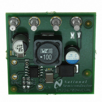
BOARD EVALUATION FOR LM22670INV
Manufacturer
National Semiconductor
Series
SIMPLE SWITCHER®r
Specifications of LM22670INVEVAL
Main Purpose
DC/DC, Step Down
Outputs And Type
1, Non-Isolated
Voltage - Output
-5V
Current - Output
1.5A
Voltage - Input
5 ~ 35V
Regulator Topology
Buck
Frequency - Switching
500kHz
Board Type
Fully Populated
Utilized Ic / Part
LM22670
Lead Free Status / RoHS Status
Not applicable / Not applicable
Power - Output
-
Other names
*LM22670INVEVAL


www.national.com
Design Considerations
Figure 1 shows the typical configuration of a polarity-inverting
converter using the LM22670 switching regulator. This invert-
ing topology design can be implemented with any member of
the LM2267X SIMPLE SWITCHER
ground pin (GND) of the LM22670 is connected to the nega-
tive output, VOUT, and the feedback resistor divider is re-
ferred to GND. No extra level shift and inversion of the
feedback signal is required to regulate the negative output
voltage. This buck-boost application is also possible with the
fixed voltage version of the LM22670 by connecting the feed-
back pin directly to ground of the system. A polarity-inverting
topology is particularly difficult to stabilize as it has a right-half
plane zero in its control to output transfer function. Two com-
pensation capacitor, C6 and C7, are connected from the input
to the negative output in order to provide more phase margin
and stabilize the loop. For output currents less than 100 mA,
the converter can be operated in discontinuous current con-
duction mode (DCM) and capacitors C6 and C7 are not
required. When capacitors C6 and C7 are used and voltage
is first applied to the application, the initial capacitor charge
current will cause a positive voltage spike on the output. This
positive voltage spike is typically too small to cause any dam-
age on the output capacitor. The initial input capacitor charge
current will cause a voltage drop across the capacitor ESR.
Since the ESR from capacitors C6 and C7 and output capac-
itors C4 and C5 form a voltage divider, the magnitude of the
initial voltage spike will be dependent upon the ESR values
of these capacitors. Since the overall output capacitor ESR
value is typically larger than the compensation capacitor ESR
value, the initial voltage spike will be typically below 500 mV.
The faster the input voltage slew rate applied to the circuit,
the larger the positive voltage spike. If the inductor DC resis-
tance is 2Ω or greater and the initial start-up current is high,
the positive voltage spike may be higher than 500 mV. An
additional clamping diode, D2, can be used in parallel to the
output capacitor C4 to clamp this positive voltage spike to
typically 300 mV if a small Schottky diode is used. Shown in
Figure 2. In most cases this clamp is not required.
FIGURE 1. Evaluation Board Schematic Inverting Topology
®
family. Note that the
2
Component Selection
This section details the component calculation and selection
for polarity-inverting converter applications. The calculations
are for continuous current conduction mode (CCM) operation.
FIGURE 2. Optional Protection Diode D2
30075202
30075201
Related parts for LM22670INVEVAL
Image
Part Number
Description
Manufacturer
Datasheet
Request
R

Part Number:
Description:
National Semiconductor [8-Bit D/A Converter]
Manufacturer:
National Semiconductor
Datasheet:
Part Number:
Description:
National Semiconductor [Media Coprocessor]
Manufacturer:
National Semiconductor
Datasheet:
Part Number:
Description:
Digitally Controlled Tone and Volume Circuit with Stereo Audio Power Amplifier, Microphone Preamp Stage and National 3D Sound
Manufacturer:
National Semiconductor
Datasheet:
Part Number:
Description:
Digitally Controlled Tone and Volume Circuit with Stereo Audio Power Amplifier, Microphone Preamp Stage and National 3D Sound
Manufacturer:
National Semiconductor
Datasheet:
Part Number:
Description:
AC97 Rev 2 Codec with Sample Rate Conversion and National 3D Sound
Manufacturer:
National Semiconductor
Part Number:
Description:
Manufacturer:
National Semiconductor
Datasheet:
Part Number:
Description:
Manufacturer:
National Semiconductor
Datasheet:
Part Number:
Description:
General Purpose, Low Voltage, Low Power, Rail-to-Rail Output Operational Amplifiers
Manufacturer:
National Semiconductor
Datasheet:
Part Number:
Description:
8-bit 20 MSPS flash A/D converter.
Manufacturer:
National Semiconductor
Datasheet:
Part Number:
Description:
Low Noise Quad Operational Amplifier
Manufacturer:
National Semiconductor
Datasheet:
Part Number:
Description:
Quad Differential Line Receivers
Manufacturer:
National Semiconductor
Datasheet:
Part Number:
Description:
Quad High Speed Trapezoidal? Bus Transceiver
Manufacturer:
National Semiconductor
Datasheet:
Part Number:
Description:
Dual Line Receiver
Manufacturer:
National Semiconductor
Datasheet:
Part Number:
Description:
TTL to 10k ECL Level Translator with Latch
Manufacturer:
National Semiconductor
Datasheet: