LM22670INVEVAL National Semiconductor, LM22670INVEVAL Datasheet - Page 3
LM22670INVEVAL
Manufacturer Part Number
LM22670INVEVAL
Description
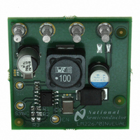
BOARD EVALUATION FOR LM22670INV
Manufacturer
National Semiconductor
Series
SIMPLE SWITCHER®r
Specifications of LM22670INVEVAL
Main Purpose
DC/DC, Step Down
Outputs And Type
1, Non-Isolated
Voltage - Output
-5V
Current - Output
1.5A
Voltage - Input
5 ~ 35V
Regulator Topology
Buck
Frequency - Switching
500kHz
Board Type
Fully Populated
Utilized Ic / Part
LM22670
Lead Free Status / RoHS Status
Not applicable / Not applicable
Power - Output
-
Other names
*LM22670INVEVAL


Inductor Selection
Duty-cycle is calculated as:
where V
drop across the LM22670 internal power N-FET. The R
(ON)
culate V
where I
average inductor current, I
load current, I
There are multiple ways to calculate the required inductance
for a switching application. The recommended calculation is
to choose the inductor ripple current, ΔI
30% of the average inductor current I
regulator operate in continuous current conduction mode
(CCM) and the application circuit will have a small load tran-
sient response with an acceptable output voltage ripple.
Therefore the peak-to-peak inductor ripple current, ΔI
lected as:
This makes the required inductance:
where F is the switching frequency of the application. The
LM22670 will switch at 500 kHz typical if the RT/SYNC pin is
floating. The inductor should have a RMS current rating equal
to or greater than the maximum current limit, I
avoid inductor saturation. The values for maximum current
limit, I
of the LM22670 datasheet.
IC Device Ratings
The DC/DC polarity-inverting converter needs to be rated for
the peak switch current, I
V
Since the ground pin, GND, of the LM22670 is connected to
the output voltage, the maximum input voltage rating has to
be able to withstand the application input voltage, V
the absolute value of output voltage, V
voltage rating of the IC is as follows:
Maximum load current, I
cycle, D, and the inductor value, L. This is important because
the LM22670 3A step-down switching regulator cannot typi-
INMAX
of the FET is specified in the LM22670 datasheet to cal-
CL
, as described below. Peak switch current is:
PEAK
, can be found in the electrical characteristics section
Q
D
according to the FET current.
is the D1 diode voltage drop and V
is the peak switch current of the application. The
OUT
, is defined as:
V
V
INMAX
Q
= I
ΔI
OUT(MAX)
PEAK
L
PEAK
= V
L
≊
, in reference to the application
0.3 x I
, and maximum input voltage,
IN
x R
, is dependent upon the duty-
+ |V
DS(ON)
L
OUT
L
,
. This will make the
OUT
|
L
, of approximately
. Maximum input
Q
CL
is the voltage
, in order to
L
IN
, is se-
, plus
DS
3
cally deliver a 3A load current in a polarity-inverting topology
as shown in Figure 3.
The formula for maximum load current in a given circuit is:
where F is the switching frequency and I
current limit threshold as specified in the electrical character-
istics section of the LM22670 datasheet.
Diode Ratings
Diode, D1, has to be able to meet the following parameters:
where I
maximum voltage rating of the diode, D1.
A Shottky diode with a low forward voltage rating is recom-
mended to achieve high converter efficiency and low EMI.
Output Capacitor Selection
The output capacitor needs to be selected primarily for a low
ESR value, but the capacitance must also be able to deliver
the maximum load current when the switch is on. The ESR
value will determine the load impedance and output voltage
ripple at the first moment diode, D1, becomes forward biased.
Thus the required ESR for a desired output voltage ripple,
ΔV
The minimum output capacitor value, C
output voltage ripple and load current is:
FIGURE 3. LM22670 Input Voltage vs Maximum Load
OUT
, is calculated as:
DMAX
is the maximum current rating and V
Current (V
V
DMAX
I
DMAX
OUT
= V
= -5V, L = 10 µH)
= I
IN
+ |V
PEAK
OUT
|,
CLMIN
OUTMIN
is the minimum
, for a desired
30075218
www.national.com
DMAX
is the
Related parts for LM22670INVEVAL
Image
Part Number
Description
Manufacturer
Datasheet
Request
R

Part Number:
Description:
National Semiconductor [8-Bit D/A Converter]
Manufacturer:
National Semiconductor
Datasheet:
Part Number:
Description:
National Semiconductor [Media Coprocessor]
Manufacturer:
National Semiconductor
Datasheet:
Part Number:
Description:
Digitally Controlled Tone and Volume Circuit with Stereo Audio Power Amplifier, Microphone Preamp Stage and National 3D Sound
Manufacturer:
National Semiconductor
Datasheet:
Part Number:
Description:
Digitally Controlled Tone and Volume Circuit with Stereo Audio Power Amplifier, Microphone Preamp Stage and National 3D Sound
Manufacturer:
National Semiconductor
Datasheet:
Part Number:
Description:
AC97 Rev 2 Codec with Sample Rate Conversion and National 3D Sound
Manufacturer:
National Semiconductor
Part Number:
Description:
Manufacturer:
National Semiconductor
Datasheet:
Part Number:
Description:
Manufacturer:
National Semiconductor
Datasheet:
Part Number:
Description:
General Purpose, Low Voltage, Low Power, Rail-to-Rail Output Operational Amplifiers
Manufacturer:
National Semiconductor
Datasheet:
Part Number:
Description:
8-bit 20 MSPS flash A/D converter.
Manufacturer:
National Semiconductor
Datasheet:
Part Number:
Description:
Low Noise Quad Operational Amplifier
Manufacturer:
National Semiconductor
Datasheet:
Part Number:
Description:
Quad Differential Line Receivers
Manufacturer:
National Semiconductor
Datasheet:
Part Number:
Description:
Quad High Speed Trapezoidal? Bus Transceiver
Manufacturer:
National Semiconductor
Datasheet:
Part Number:
Description:
Dual Line Receiver
Manufacturer:
National Semiconductor
Datasheet:
Part Number:
Description:
TTL to 10k ECL Level Translator with Latch
Manufacturer:
National Semiconductor
Datasheet: