SI3452MS8-KIT Silicon Laboratories Inc, SI3452MS8-KIT Datasheet - Page 32
SI3452MS8-KIT
Manufacturer Part Number
SI3452MS8-KIT
Description
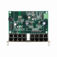
BOARD EVAL FOR SI3452
Manufacturer
Silicon Laboratories Inc
Type
Controllers & Processorsr
Specifications of SI3452MS8-KIT
Main Purpose
Special Purpose DC/DC, Power Over Ethernet
Board Type
Fully Populated
Utilized Ic / Part
Si3452
Interface Type
Ethernet, USB, I2C
Operating Voltage
3.3 V
Operating Temperature Range
- 40 C to + 85 C
Product
Modules
For Use With/related Products
Si3452
Lead Free Status / RoHS Status
Lead free / RoHS Compliant
Current - Output
-
Voltage - Output
-
Voltage - Input
-
Power - Output
-
Frequency - Switching
-
Outputs And Type
-
Regulator Topology
-
Lead Free Status / Rohs Status
Lead free / RoHS Compliant
Other names
336-1836


Si3452
11. Recommended PCB Footprint
32
Notes:
General
Solder Mask Design
Stencil Design
Card Assembly
1. All dimensions shown are in millimeters (mm) unless otherwise noted.
2. Dimensioning and Tolerancing is per the ANSI Y14.5M-1994 specification.
3. This Land Pattern Design is based on IPC-SM-782 guidelines.
4. All dimensions shown are at Maximum Material Condition (MMC). Least Material Condition
5. All metal pads are to be non-solder mask defined (NSMD). Clearance between the solder
6. A stainless steel, laser-cut and electro-polished stencil with trapezoidal walls should be used
7. The stencil thickness should be 0.125 mm (5 mils).
8. The ratio of stencil aperture to land pad size should be 1:1 for the perimeter pads.
9. A 4x4 array of 0.80 mm square openings on 1.05 mm pitch should be used for the center Vee
10. A No-Clean, Type-3 solder paste is recommended.
11. The recommended card reflow profile is per the JEDEC/IPC J-STD-020 specification for Small
(LMC) is calculated based on a Fabrication Allowance of 0.05 mm.
mask and the metal pad is to be 60 µm minimum, all the way around the pad.
to assure good solder paste release.
pad.
Body Components.
Dimension
GE
GD
D2
ZE
ZD
E2
E
D
X
Y
e
Table 27. PCB Land Pattern Dimensions
Figure 8. PCB Land Pattern
Rev. 1.2
4.00
4.00
4.53
4.53
Min
—
—
—
0.50 BSC
0.89 REF
5.42 REF
5.42 REF
Max
4.20
4.20
0.28
6.31
6.31
—
—
Related parts for SI3452MS8-KIT
Image
Part Number
Description
Manufacturer
Datasheet
Request
R

Part Number:
Description:
SMD/C°/SINGLE-ENDED OUTPUT SILICON OSCILLATOR
Manufacturer:
Silicon Laboratories Inc
Part Number:
Description:
Manufacturer:
Silicon Laboratories Inc
Datasheet:
Part Number:
Description:
N/A N/A/SI4010 AES KEYFOB DEMO WITH LCD RX
Manufacturer:
Silicon Laboratories Inc
Datasheet:
Part Number:
Description:
N/A N/A/SI4010 SIMPLIFIED KEY FOB DEMO WITH LED RX
Manufacturer:
Silicon Laboratories Inc
Datasheet:
Part Number:
Description:
N/A/-40 TO 85 OC/EZLINK MODULE; F930/4432 HIGH BAND (REV E/B1)
Manufacturer:
Silicon Laboratories Inc
Part Number:
Description:
EZLink Module; F930/4432 Low Band (rev e/B1)
Manufacturer:
Silicon Laboratories Inc
Part Number:
Description:
I°/4460 10 DBM RADIO TEST CARD 434 MHZ
Manufacturer:
Silicon Laboratories Inc
Part Number:
Description:
I°/4461 14 DBM RADIO TEST CARD 868 MHZ
Manufacturer:
Silicon Laboratories Inc
Part Number:
Description:
I°/4463 20 DBM RFSWITCH RADIO TEST CARD 460 MHZ
Manufacturer:
Silicon Laboratories Inc
Part Number:
Description:
I°/4463 20 DBM RADIO TEST CARD 868 MHZ
Manufacturer:
Silicon Laboratories Inc
Part Number:
Description:
I°/4463 27 DBM RADIO TEST CARD 868 MHZ
Manufacturer:
Silicon Laboratories Inc
Part Number:
Description:
I°/4463 SKYWORKS 30 DBM RADIO TEST CARD 915 MHZ
Manufacturer:
Silicon Laboratories Inc
Part Number:
Description:
N/A N/A/-40 TO 85 OC/4463 RFMD 30 DBM RADIO TEST CARD 915 MHZ
Manufacturer:
Silicon Laboratories Inc
Part Number:
Description:
I°/4463 20 DBM RADIO TEST CARD 169 MHZ
Manufacturer:
Silicon Laboratories Inc