NCP1230GEVB ON Semiconductor, NCP1230GEVB Datasheet - Page 4
NCP1230GEVB
Manufacturer Part Number
NCP1230GEVB
Description
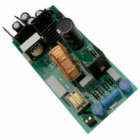
EVAL BOARD FOR NCP1230G
Manufacturer
ON Semiconductor
Specifications of NCP1230GEVB
Design Resources
NCP1230 EVB BOM NCP1230GEVB Gerber Files NCP1230 EVB Schematic
Main Purpose
AC/DC, Primary Side
Outputs And Type
1, Isolated
Power - Output
90W
Voltage - Output
18.6V
Current - Output
4.74A
Voltage - Input
85 ~ 265VAC
Regulator Topology
Flyback
Frequency - Switching
47kHz
Board Type
Fully Populated
Utilized Ic / Part
NCP1230
Lead Free Status / RoHS Status
Lead free / RoHS Compliant
For Use With/related Products
NCP1230G
Other names
NCP1230GEVBOS


Where:
following equation. See Application Note AN1679/D for
details of how the snubber equations were derived.
values were tuned in the circuit to minimize ringing, and
minimize the power dissipation. As a result the final circuit
values are; Rclamp uses three 100 kW (33 kW equivalent),
2.0 W resistors used in parallel, and C6 is 0.01 mF, 1000 V.
Refer to Figure 1 for a scope waveform of the Drain to source
voltage at full load and high line.
Current Sense Resistor Selection
1.0 V (typical). The current sense resistor should be
calculated at 125% of the full rated load to be sure that under
all operating conditions the power supply will be able to
deliver the full rated power.
PRclamp + 0.5 · Ipk 2 · le · Freq ·
PRclamp + 0.5 · 3.97 2 · 7 · 65 ·
Vo = the output voltage
Vf = the forward voltage drop across the output diode
n is the transformer turns ratio 6.77
Ie is the transformer turns ratio of 7 mH
The power dissipation in the clamp resistor is:
The snubber capacitor can be calculated from the
After the initial snubber was calculated, the snubber
The input to the current sense amplifier is clamped to
+ 4.4 W
Pin + Po
Ipk +
C6 +
C6 +
Po + 90 · 1.25 + 112.5 W
20 · 65 · 110
eff
Vripple · Freq · Rclamp
2 · 140.63
220 · 65
+ 112.5
Figure 1.
700
0.80
Vclamp
+ 140.63 W
+ 4.43 Apk
+ 0.005 mF
700 * ( 19.7 · 6.77 )
Vclamp * ( Vo · n )
Vclamp
700
http://onsemi.com
AND8154/D
4
0.2 W was used.
0.4 W resistors were used in parallel.
Overvoltage Protection
the current sense pin during the power switch off time. If the
voltage on the current sense pin rises above 3.0 V (typical),
the NCP1230 will immediately stop the output drive pulses
and latch−off the controller. The NCP1230 will stay in the
Latch−Off mode until Vcc has dropped below 4.0 V.
protection functions, for example, Overvoltage or
Overtemperature Protection.
can be used for overvoltage protection because the voltage
on the Auxiliary winding is proportional to the output
voltage.
transistor is used to bias up the current sense pin during the
NCP1230 controller off time (refer to Figure 2). The base of
the PNP transistor is driven by the NCP1230 drive output
(pin 5), if the Auxiliary winding voltage increases above the
Zener diode (D1) breakdown voltage, 13 V, current will
flow through Q3 biasing up the voltage on the current sense
pin. Using typical component values, if the voltage on the
Auxiliary winding reaches 16.5 V (3.5 V above the nominal
voltage) the NCP1230 will latch−off through the CS input
(pin 3).
Latch−Off prior to having Vcc reach its maximum allowable
voltage level, 18 V.
To reduce the power dissipation in the sense resistor, two
The NCP1230 has a fast comparator which only monitors
This feature allows the user to implement several
The Auxiliary winding of the Flyback transformer (T5)
To implement Overvoltage Protection (OVP), a PNP
A 13 V Zener diode was selected to have the controller
OVPthreshold + Vz(D1) ) VceQ3 ) CSlatchoff
10 k
Figure 2. Overvoltage Protection Circuit
Vaux
Rs + 1 V
100 pF
MMBT2907A/SOT
13 V
+ 13 V ) 0.5 V ) 3.0 V + 16.5 V
Ipk
+ 1
4.43
+ 0.23 W
1
2
3
4
1 k
GTS
FB
CS
GND
NCP1230
VCC
DRV
HV
Rsense
8
6
5
Related parts for NCP1230GEVB
Image
Part Number
Description
Manufacturer
Datasheet
Request
R

Part Number:
Description:
Fixed Frequency Controller Featuring Pfc Go To Standby Function
Manufacturer:
ON Semiconductor
Datasheet:
Part Number:
Description:
ON Semiconductor [VOLTAGE REGULATOR]
Manufacturer:
ON Semiconductor
Datasheet:
Part Number:
Description:
357-036-542-201 CARDEDGE 36POS DL .156 BLK LOPRO
Manufacturer:
ON Semiconductor
Datasheet:
Part Number:
Description:
357-036-542-201 CARDEDGE 36POS DL .156 BLK LOPRO
Manufacturer:
ON Semiconductor
Datasheet:
Part Number:
Description:
357-036-542-201 CARDEDGE 36POS DL .156 BLK LOPRO
Manufacturer:
ON Semiconductor
Datasheet:
Part Number:
Description:
357-036-542-201 CARDEDGE 36POS DL .156 BLK LOPRO
Manufacturer:
ON Semiconductor
Datasheet:
Part Number:
Description:
357-036-542-201 CARDEDGE 36POS DL .156 BLK LOPRO
Manufacturer:
ON Semiconductor
Datasheet:
Part Number:
Description:
357-036-542-201 CARDEDGE 36POS DL .156 BLK LOPRO
Manufacturer:
ON Semiconductor
Datasheet:
Part Number:
Description:
357-036-542-201 CARDEDGE 36POS DL .156 BLK LOPRO
Manufacturer:
ON Semiconductor
Datasheet:
Part Number:
Description:
357-036-542-201 CARDEDGE 36POS DL .156 BLK LOPRO
Manufacturer:
ON Semiconductor
Datasheet:
Part Number:
Description:
357-036-542-201 CARDEDGE 36POS DL .156 BLK LOPRO
Manufacturer:
ON Semiconductor
Datasheet:
Part Number:
Description:
357-036-542-201 CARDEDGE 36POS DL .156 BLK LOPRO
Manufacturer:
ON Semiconductor
Datasheet:
Part Number:
Description:
Manufacturer:
ON Semiconductor
Datasheet:
Part Number:
Description:
Manufacturer:
ON Semiconductor
Datasheet: