EVALSF2-ICE2A0565Z-12 Infineon Technologies, EVALSF2-ICE2A0565Z-12 Datasheet - Page 7
EVALSF2-ICE2A0565Z-12
Manufacturer Part Number
EVALSF2-ICE2A0565Z-12
Description
BOARD DEMO ICE2A0565Z 10W SMPS
Manufacturer
Infineon Technologies
Series
CoolSET®F2r
Specifications of EVALSF2-ICE2A0565Z-12
Main Purpose
AC/DC, Primary Side
Outputs And Type
1, Isolated
Power - Output
10W
Voltage - Output
5V
Current - Output
2A
Voltage - Input
85 ~ 270VAC
Regulator Topology
Flyback
Frequency - Switching
100kHz
Board Type
Fully Populated
Utilized Ic / Part
ICE2A0565
Lead Free Status / RoHS Status
Lead free / RoHS Compliant
Other names
EVALSF2-ICE2A0565Z-12IN


Description
Introduction
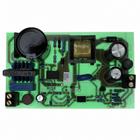
The EVALSF2-ICE2A0565Z demoboard is a low cost off line flyback switch mode power supply
(SMPS) using the ICE2A0565Z system IC from the CoolSET
2
265V
Line Input
The AC line input side comprises of an input fuse F1 as line input over current protection as well as
choke L5 and the X2 capacitor C8 as radio interference suppressors. After the bridge rectifier BR1
and input capacitor C3, a voltage from 120 to 380 V
of the ICE-F2-family there is the possibility to replace the 47µF input capacitor with a 22µF (2.2µF/W)
Startup
From this voltage, the chip starting the current supply is derived using resistors R6 and R7. Because
of the very low start up current of typically 27µA, a high-value resistor can be used.
Operation Mode
During operation, the V
rectification D2 and buffering C4, C13. Resistor R8 is used for current limiting during the charging of
C4. In order not to exceed the maximum voltage at V
voltage. During light or no load condition, the switching frequency is automatically and continuously
reduced down to 21kHz
Softstart
The Soft-Start function is realized by an internal resistor and the adjustable external capacitor C14.
Snubber Network
The network R10, C12 and D3 clamp the DRAIN voltage spike caused by transformer leakage
inductance to a safe value below the drain source break down voltage V
Limitation of primary current
The CoolMOS drain source current is sensed via external shunt resistors R17. An accurate value of
the shunt improves the peak power limitation shown in the curve peak power limitation in the rear of
this report.
Output Voltage
Power is coupled out on the secondary side via a fast-acting diode D1 with low forward voltage.
Capacitor C5 performs energy buffering, a following LC - filter C9 and inductor L3 considerably
reduces the output voltage ripple. Storage output capacitor C5 is designed to exhibit a very low ESR in
order to minimize the output voltage ripple caused by the triangular 100kHz current characteristic. The
output voltage is set with resistors R1 and R2.
Regulation
The output voltage is controlled using a type TL431 reference diode (IC2). This device incorporates
the voltage reference as well as the error amplifier and a driver stage. Compensation network C1, C2,
R1, R5 constitutes the external circuitry of the error amplifier of IC2. This circuitry allows the feedback
to be precisely matched to dynamically varying load conditions, thereby providing stable control. The
maximum current through the optocoupler diode and the voltage reference is set by using resistors
R3, R4. Optocoupler IC1 is used for floating transmission of the control signal to the “Feedback” input
via resistor R9 and capacitor C6 of the ICE2A0565Z control device. The optocoupler used meets DIN
VDE 884 requirements for a wider creepage distance.
3
4
5
www.Infineon.com/CoolSET
, details a 5.0V, 10W power supply that operates from an AC line input voltage range of 85 to
Slope Compensation is needed due to Current Mode Control and Dnom > 50% see description in the rear of the report
Without audible noise
V
DSBR
AC
, suitable for applications requiring either an open frame supply or an enclosed adapter.
= 650V @ Tj = 110°C
CC
4
in order to reduce the switching losses.
pin is supplied via a separate transformer winding with associated
10W 5V Demoboard using ICE2A0565Z on Board
Page 6 of 16
DC
CC
is present. Due to the extended duty cycle D
pin an external zener diode D4 limits this
-F2 family. The circuit, shown in
DSBR
= 650V
EVALSF2-ICE2A0565Z
5
maximum.
Figure
V2.00
MAX
3
.
Related parts for EVALSF2-ICE2A0565Z-12
Image
Part Number
Description
Manufacturer
Datasheet
Request
R

Part Number:
Description:
Manufacturer:
Infineon Technologies AG
Datasheet:
Part Number:
Description:
Manufacturer:
Infineon Technologies AG
Datasheet:
Part Number:
Description:
Manufacturer:
Infineon Technologies AG
Datasheet:
Part Number:
Description:
Manufacturer:
Infineon Technologies AG
Datasheet:
Part Number:
Description:
Manufacturer:
Infineon Technologies AG
Datasheet:
Part Number:
Description:
Manufacturer:
Infineon Technologies AG
Datasheet:
Part Number:
Description:
Manufacturer:
Infineon Technologies AG
Datasheet:
Part Number:
Description:
16-bit microcontroller with 2x2 KByte RAM
Manufacturer:
Infineon Technologies AG
Datasheet:
Part Number:
Description:
NPN silicon RF transistor
Manufacturer:
Infineon Technologies AG
Datasheet:
Part Number:
Description:
NPN silicon RF transistor
Manufacturer:
Infineon Technologies AG
Datasheet:
Part Number:
Description:
NPN silicon RF transistor
Manufacturer:
Infineon Technologies AG
Datasheet:
Part Number:
Description:
NPN silicon RF transistor
Manufacturer:
Infineon Technologies AG
Datasheet:
Part Number:
Description:
Si-MMIC-amplifier in SIEGET 25-technologie
Manufacturer:
Infineon Technologies AG
Datasheet:
Part Number:
Description:
IGBT Power Module
Manufacturer:
Infineon Technologies AG
Datasheet:
Part Number:
Description:
IC for switching-mode power supplies
Manufacturer:
Infineon Technologies AG
Datasheet: