NCP1605FORWGEVB ON Semiconductor, NCP1605FORWGEVB Datasheet
NCP1605FORWGEVB
Manufacturer Part Number
NCP1605FORWGEVB
Description
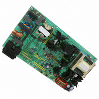
EVAL BOARD FOR NCP1605FORWG
Manufacturer
ON Semiconductor
Datasheets
1.NCP1217P100G.pdf
(19 pages)
2.NCP1605ADR2G.pdf
(32 pages)
3.NCP1605FORWGEVB.pdf
(2 pages)
4.NCP1605FORWGEVB.pdf
(20 pages)
Specifications of NCP1605FORWGEVB
Design Resources
NCP1605FORWGEVB BOM NCP1605FORWGEVB Gerber Files NCP1605 EVB Schematic
Main Purpose
AC/DC, Primary and Secondary Side with PFC
Outputs And Type
1, Isolated
Voltage - Output
19V
Current - Output
8A
Voltage - Input
90 ~ 265VAC
Regulator Topology
Forward Converter
Frequency - Switching
133kHz
Board Type
Fully Populated
Utilized Ic / Part
NCP1217, NCP1605
Lead Free Status / RoHS Status
Lead free / RoHS Compliant
Power - Output
-
Lead Free Status / Rohs Status
Lead free / RoHS Compliant
For Use With/related Products
NCP1605FORWG
Other names
NCP1605FORWGEVBOS


7/31/2007
1.
2.
3.
4.
Test Procedure for the NCP1605 Forward Evaluation Board
Apply a resistive or an active load across the output (between the “+V
load must be able to draw 12 A from 19 V (use a 25 V or more voltage load for a safe headroom).
To evaluate the board performance, it is recommended to place a power analyzer able to measure:
As portrayed by figure 1, this power-meter should be inserted between the power source and the board (the power
source being defined in next point).
Plug the application to a 250 W or more, isolated ac power source. This source that is applied, is supposed to simulate
the line utility. Hence, the power source voltage should be a 50 or 60 Hz sinusoid (without dc component). Its
magnitude must remain below 265 Vrms.
You can them measure the board performance presented in ANDxxxx. Among them, we can list:
•
•
•
•
•
The power delivered by the power source (“Pin”),
The power factor (“PF”) and the Total Harmonic Distortion (“THD”) of the current absorbed from the ac
power source.
Apply 120 Vrms and load the output with 8 A
Decrease the load current. When I
can check it by observing the line current that must be bursting.
Increase the load current until 19 V output voltage drops. The load current should be less than 12 A and the
power supply should be hiccupping. Again, you can check this by observing the line current. This test must
be very short to avoid any excessive heating of the board (designed for I
if the power supply does not enter hiccup mode while I
iii. The input power should be less than 190 W
ii. The power factor should be higher than 0.990
i. The output voltage should be between 18.5 and 19.5 V.
Figure 1 – Board connection
Test Procedure
OUT
is below 0.25 A, the PFC stage should have entered skip mode. You
OUT
is 12 A.
OUT
” and “-V
OUT
OUT
= 8 A). Immediately stop the test
” terminals of the board). This
Related parts for NCP1605FORWGEVB
Image
Part Number
Description
Manufacturer
Datasheet
Request
R

Part Number:
Description:
ON Semiconductor [VOLTAGE REGULATOR]
Manufacturer:
ON Semiconductor
Datasheet:
Part Number:
Description:
357-036-542-201 CARDEDGE 36POS DL .156 BLK LOPRO
Manufacturer:
ON Semiconductor
Datasheet:
Part Number:
Description:
357-036-542-201 CARDEDGE 36POS DL .156 BLK LOPRO
Manufacturer:
ON Semiconductor
Datasheet:
Part Number:
Description:
357-036-542-201 CARDEDGE 36POS DL .156 BLK LOPRO
Manufacturer:
ON Semiconductor
Datasheet:
Part Number:
Description:
357-036-542-201 CARDEDGE 36POS DL .156 BLK LOPRO
Manufacturer:
ON Semiconductor
Datasheet:
Part Number:
Description:
357-036-542-201 CARDEDGE 36POS DL .156 BLK LOPRO
Manufacturer:
ON Semiconductor
Datasheet:
Part Number:
Description:
357-036-542-201 CARDEDGE 36POS DL .156 BLK LOPRO
Manufacturer:
ON Semiconductor
Datasheet:
Part Number:
Description:
357-036-542-201 CARDEDGE 36POS DL .156 BLK LOPRO
Manufacturer:
ON Semiconductor
Datasheet:
Part Number:
Description:
357-036-542-201 CARDEDGE 36POS DL .156 BLK LOPRO
Manufacturer:
ON Semiconductor
Datasheet:
Part Number:
Description:
357-036-542-201 CARDEDGE 36POS DL .156 BLK LOPRO
Manufacturer:
ON Semiconductor
Datasheet:
Part Number:
Description:
357-036-542-201 CARDEDGE 36POS DL .156 BLK LOPRO
Manufacturer:
ON Semiconductor
Datasheet:
Part Number:
Description:
Manufacturer:
ON Semiconductor
Datasheet:
Part Number:
Description:
Manufacturer:
ON Semiconductor
Datasheet:
Part Number:
Description:
Manufacturer:
ON Semiconductor
Datasheet:
NCP1605FORWGEVB Summary of contents
Page 1
Test Procedure for the NCP1605 Forward Evaluation Board 7/31/2007 1. Apply a resistive or an active load across the output (between the “+V load must be able to draw 12 A from 19 V (use more ...
Page 2
Input socket with earth The board contains high voltage, hot, live parts. Only persons skilled in the art of power electronics should manipulate or test it. Be very cautious when doing so the responsibility of those who receive ...