NCP1605FORWGEVB ON Semiconductor, NCP1605FORWGEVB Datasheet
NCP1605FORWGEVB
Specifications of NCP1605FORWGEVB


Related parts for NCP1605FORWGEVB

NCP1605FORWGEVB Summary of contents
Page 1
... AND8292 Wide Mains Power Supply Including Power Factor Correction Prepared by: Joël Turchi, ON Semiconductor Introduction When associated to forward or half-bridge converters taking advantage of a narrow input voltage range, the PFC stage should be designed to start first and to remain active as long as the power supply is plugged in. More specifically, the downstream converter turns on and operates while the output of the PFC stage is nominal ...
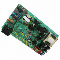
Page 2
AND8292 Figure 1. The Board http://onsemi.com 2 ...
Page 3
AND8292 Figure 2. Application Schematic - PFC Stage http://onsemi.com 3 ...
Page 4
AND8292 Figure 3. Application Schematic - 2 Switch Forward Converter http://onsemi.com 4 ...
Page 5
AND8292 Figure 4. PCB Layout - Silkscreen Top Figure 5. PCB Layout - Silkscreen Bottom http://onsemi.com 5 ...
Page 6
AND8292 Figure 6. PCB Layout - Bottom Layer http://onsemi.com 6 ...
Page 7
AC Line Current (5 A/div (CH1) BULK V = 120 V, Pin = 183 W, I IN,RMS : AC Line Current (5 A/div (CH1) BULK V (CH3) BULK V = 230 V, Pin ...
Page 8
Table 1. Power Factor and Efficiency V P IN, RMS IN, AVG (V) (W) 90 28.2 0.966 90 70.5 0.991 90 114.5 0.995 90 183.2 0.990 120 27.7 0.961 120 70.3 0.987 120 113.2 0.992 120 180.3 0.997 230 28.0 ...
Page 9
Startup Sequencing at 120 Vrms and I Load Current (5 A/div) Figure 8. Startup Phase at 120 Vrms and I When the PFC output voltage (V nominal voltage (about 382 V), the circuit detects the end of AND8292 = 8 ...
Page 10
We can note some skipping sequence that takes place after «pfcOK» has turned high. This is because the NCP1605 standby management block is controlled by the feedback signal of the main converter. The PFC stage recovers activity AND8292 Load Current ...
Page 11
Compared to the precedent one, Figure 10 further shows the 19 V output. Overload / Short Circuit Protections The application embeds a circuitry (see Figure 13) to detect overload conditions. A buffer (Q1x) builds a low impedance signal that is ...
Page 12
AC Line Current (2 A/div) V (100 V/div) BULK VI (100 V/div) N Figure 11. The Circuit Enters a Safe Low Duty-Cycle Hiccup Mode if the 19 V Output is Short Circuited AND8292 (Test Made at 120 V ) RMS ...
Page 13
More generally, this protection triggers when the load current (I Table 2. V (V) IN, RMS I (A) OUT When Q3 is on, V goes low and cannot be generated any more. The application enters hiccup mode. ...
Page 14
Protection of the PFC Stages The NCP1605 protection features allow the design of very rugged PFC stages: • The following brownout detection levels were measured (the 19 V output being loaded current): - Minimum line RMS ...
Page 15
Dynamic Performance The following plots were obtained by varying (slope 2 A/ms) at 120 Vrms. One can note that thanks to the NCP1605 dynamic response enhancer, the bulk voltage stays largely above I I ...
Page 16
V (100 V/div) IN Standby Performance In light load conditions, the circuit enters skip mode to reduce the losses (the PFC stage remaining on in stand-by Table IN, AVG (No Load) *These values were obtained by ...
Page 17
AND8292 I (5 A/div) OUT V (100 V/div) IN Figure 17. Skip Mode Operation of the PFC Stage at 120 Vrms, No Load. The Skip Mode Period is About 1 A/div) OUT 382 V Figure 18. Zoom ...
Page 18
AND8292 I (5 A/div) OUT V (100 V/div) BULK V (100 V/div) IN Figure 19. Skip Mode Operation of the PFC Stage at 230 Vrms, No Load A/div) (5 A/div) OUT OUT 382 V V (100 V/div) ...
Page 19
... Output Diodes (MBR20100) Output Coil 100°C 110°C EPCOS Wurth Electronik RIFA BC Components various various various various various various muRata Nichicon various various various various various various ON Semiconductor various ON Semiconductor ON Semiconductor ON Semiconductor ON Semiconductor ON Semiconductor ON Semiconductor ON Semiconductor Schaffner Schaffner CoilCraft Infineon ON Semiconductor ...
Page 20
... Opportunity/Affirmative Action Employer. This literature is subject to all applicable copyright laws and is not for resale in any manner. PUBLICATION ORDERING INFORMATION LITERATURE FULFILLMENT: Literature Distribution Center for ON Semiconductor P.O. Box 5163, Denver, Colorado 80217 USA Phone: 303-675-2175 or 800-344-3860 Toll Free USA/Canada Fax: 303-675-2176 or 800-344-3867 Toll Free USA/Canada ...