STEVAL-SPDC01V1 STMicroelectronics, STEVAL-SPDC01V1 Datasheet
STEVAL-SPDC01V1
Specifications of STEVAL-SPDC01V1


Related parts for STEVAL-SPDC01V1


STEVAL-SPDC01V1 Summary of contents
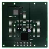
Page 1
Features ■ Complete switch mode power supply ■ max output current ■ Input voltage range from 1 ■ Supply voltage range from 4 ■ Fixed or adjustable output voltage range ...
Page 2
Contents Contents 1 Description . . . . . . . . . . . . . . . . . . . . . . . . . . . . . . . . . . . . ...
Page 3
SPDC12L00010 5.18 Input capacitors . . . . . . . . . . . . . . . . . . . . . . . . . . . . . . . . . . . . ...
Page 4
Description 1 Description The ST SPDC12L00010 high density 10 A DC-DC converter is a complete step-down power supply. A single LGA package includes ST switching controller, power FETs, inductor and all the support components. SPDC12L00010 operates over a wide input ...
Page 5
SPDC12L00010 2 Pin settings 2.1 Pin connection and mechanical data (dimensions in mm) Figure 1. Pin connection 2.2 Pin description Table 2. Pin description Name Function J11 VAUX K11 OS L2 VSENSE L3 VCC Auxiliary voltage. Internally regulated 5 V ...
Page 6
Pin settings Table 2. Pin description (continued) Name Function PGDLY L6 SYNC L7 PRG L8 SGND L9 FB L10 COMP L11 SS_INL Bank 1 VIN Bank 2 PGND Bank 3 VOUT Bank 4 PH 6/29 Power Good. ...
Page 7
SPDC12L00010 3 Maximum ratings 3.1 Absolute maximum ratings Table 3. Absolute maximum ratings Symbol SGND and PGND K11 V VSENSE to SGND and PGND L2 V VCC to SGND and PGND SGND and ...
Page 8
Maximum ratings 3.3 Thermal de-rating The thermal de-rating is obtained reducing the maximum output current, to limit the module temperature to the maximum allowable value. Since a lot of parameters affect the module power dissipation, the best way to get ...
Page 9
SPDC12L00010 Table 5. Thermal de-rating for Vout = 5.0 V Symbol Parameter Test condition Output current ...
Page 10
Maximum ratings Table 6. Thermal de-rating for Vout = 3.3 V Symbol 10/29 Parameter Test condition Output current ...
Page 11
SPDC12L00010 Table 7. Thermal de-rating for Vout = 2.5 V Symbol Parameter Test condition Output current ...
Page 12
Maximum ratings Table 8. Thermal de-rating for Vout = 1.8 V Symbol 12/29 Parameter Test condition Output current ...
Page 13
SPDC12L00010 Table 9. Thermal de-rating for Vout = 1.2 V Symbol Parameter Test condition Output current ...
Page 14
Maximum ratings Table 10. Thermal de-rating for Vout = 0.7 V Symbol 14/29 Parameter Test condition Output current ...
Page 15
SPDC12L00010 4 Electrical characteristics Table 11. Electrical characteristics Symbol Parameter V Ripple voltage r I Output current o I Current limit ol I Total quiescent current q I Total stand-by quiescent current qst- quiescent current CCq CC I ...
Page 16
Electrical characteristics 4.1 Typical performance characteristics Figure 3. Efficiency versus load current with V 100 Eff.[%] 0.0 Figure 4. Efficiency versus load current with V 100 Eff.[%] 0.0 ...
Page 17
SPDC12L00010 5 Application information 5.1 Input voltage There are two voltage supply pins: VCC (pin L3), for controller voltage supply; VIN (bank 1), for power circuit voltage supply. VCC and VIN can be connected and supplied together; if VIN is ...
Page 18
Application information 5.4 Soft-start The soft-start phase begins when both VCC and VIN raise above their turn-on thresholds, otherwise the SS_INL pin is internally shorted to SGND. A ramp is generated at SS_INL pin during start-up, charging the external capacitor ...
Page 19
SPDC12L00010 5.6 Power Good signal and Power Good delay The output voltage is monitored by FB (pin L9 not within ± 10% (typ.) of the programmed value, the PG (pin L4) output is forced low. The PG ...
Page 20
Application information 5.9 Undervoltage lock out Connecting a proper resistor (see par. is possible to select two different thresholds for UVLO: 4.2 V/3.8 V for 5 V input range; 8.6 V/7.7 V for 12 V input range. 5.10 Program setting ...
Page 21
SPDC12L00010 Figure 6. Voltage sensing 5.12 Output voltage programming Adding a resistor Rx between FB (pin L9) and SGND (L8) or between FB and VSENSE (pin L2 possible to change the output voltage. Connecting the resistor to SGND ...
Page 22
Application information Figure 8. Additional loop compensation 5.14 Output over voltage protection The device provides OVP: when the voltage sensed on FB (pin L9) reaches a value greater than 20% of reference, the on module low side driver is turned ...
Page 23
SPDC12L00010 5.16 Thermal shutdown When the controller junction temperature reaches 150 ± 10 °C, the device shutdown. Both MOSFET are turned OFF and the soft-start capacitor is discharged. The device does not restart until the junction temperature goes down to ...
Page 24
Application information 5.20 Phase connection On the module bottom, there is an area relative to PH (bank 4) connection: this area is internally connected to the high side MOSFET source and to the low side MOSFET drain; this electrical point ...
Page 25
SPDC12L00010 6 Package mechanical data In order to meet environmental requirements, ST offers these devices in different grades of ® ECOPACK packages, depending on their level of environmental compliance. ECOPACK® specifications, grade definitions and product status are available at: www.st.com. ...
Page 26
Package mechanical data 6.1 Soldering Soldering phase has to be execute with care: in order to avoid undesired melting phenomenon, particular attention has to be take on the set up of the peak temperature. Here following some suggestions for the ...
Page 27
SPDC12L00010 6.2 PCB footprint Use Figure 12 as suggested PCB footprint. Figure 12. PCB footprint top side - through view for SPDC12L00010 (mm) Doc ID 15103 Rev 3 Package mechanical data 27/29 ...
Page 28
Revision history 7 Revision history Table 14. Document revision history Date 25-Nov-2008 19-Jan-2009 02-Sep-2009 28/29 Revision 1 First release 2 Updated coverpage, 3 Updated coverpage, Doc ID 15103 Rev 3 SPDC12L00010 Changes Chapter 3.3 on page 8 Chapter 1 on ...
Page 29
... SPDC12L00010 Information in this document is provided solely in connection with ST products. STMicroelectronics NV and its subsidiaries (“ST”) reserve the right to make changes, corrections, modifications or improvements, to this document, and the products and services described herein at any time, without notice. All ST products are sold pursuant to ST’s terms and conditions of sale. ...