LM5007SD-EVAL National Semiconductor, LM5007SD-EVAL Datasheet - Page 5
LM5007SD-EVAL
Manufacturer Part Number
LM5007SD-EVAL
Description
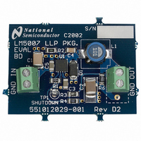
EVALUATION BOARD FOR LM5007SD
Manufacturer
National Semiconductor
Specifications of LM5007SD-EVAL
Main Purpose
DC/DC, Step Down
Outputs And Type
1, Non-Isolated
Voltage - Output
10V
Current - Output
400mA
Voltage - Input
12 ~ 75V
Regulator Topology
Buck
Board Type
Fully Populated
Utilized Ic / Part
LM5007
Lead Free Status / RoHS Status
Not applicable / Not applicable
Power - Output
-
Frequency - Switching
-
Other names
*LM5007SD EVAL
*LM5007SD-EVAL
LM5007SD EVAL
LM5007SDEVAL
LM5007SDEVAL
*LM5007SD-EVAL
LM5007SD EVAL
LM5007SDEVAL
LM5007SDEVAL


Minimum Off Time
Regulation and OV Comparators
Thermal Shutdown
Tsd
Thermal Resistance
θ
JA
Note 1: Absolute Maximum Ratings are limits beyond which damage to the device may occur. Operating Ratings are conditions under which operation of the
device is intended to be functional. For guaranteed specifications and test conditions, see the Electrical Characteristics.
Note 2: For detailed information on soldering plastic MSOP and LLP packages, refer to the Packaging Data Book available from National Semiconductor
Corporation.
Note 3: All limits are guaranteed. All electrical characteristics having room temperature limits are tested during production with T
limits are guaranteed by correlating the electrical characteristics to process and temperature variations and applying statistical process control.
Note 4: The V
Note 5: The human body model is a 100pF capacitor discharge through a 1.5kΩ resistor into each pin. The machine model is a 200pF capacitor discharged
directly into each pin. The machine model ESD compliance level for Pin 5 is 150V. The human body ESD compliance level for Pin 7 and 8 is 1000V.
Note 6: For devices procurred in the LLP-8 package the Rds(on) limits are guaranteed by design characterization data only.
Symbol
CC
Minimum Off Timer
FB Reference Threshold
FB Over-Voltage Threshold
FB Bias Current
Thermal Shutdown Temp.
Thermal Shutdown Hysteresis
Junction to Ambient
output is intended as a self bias for the internal gate drive power and control circuits. Device thermal limitations limit external loading.
Parameter
FB = 0V
Internal reference
Trip point for switch ON
Trip point for switch OFF
MUA Package
SDC Package
Conditions
5
2.445
Min
2.875
Typ
300
100
165
200
2.5
25
40
A
= T
2.550
Max
J
= 25°C. All hot and cold
www.national.com
Units
°C/W
°C/W
nA
°C
°C
ns
V
V
Related parts for LM5007SD-EVAL
Image
Part Number
Description
Manufacturer
Datasheet
Request
R

Part Number:
Description:
IC BUCK ADJ .5A 8LLP
Manufacturer:
National Semiconductor
Datasheet:


Part Number:
Description:
National Semiconductor [8-Bit D/A Converter]
Manufacturer:
National Semiconductor
Datasheet:
Part Number:
Description:
National Semiconductor [Media Coprocessor]
Manufacturer:
National Semiconductor
Datasheet:
Part Number:
Description:
Digitally Controlled Tone and Volume Circuit with Stereo Audio Power Amplifier, Microphone Preamp Stage and National 3D Sound
Manufacturer:
National Semiconductor
Datasheet:
Part Number:
Description:
Digitally Controlled Tone and Volume Circuit with Stereo Audio Power Amplifier, Microphone Preamp Stage and National 3D Sound
Manufacturer:
National Semiconductor
Datasheet:
Part Number:
Description:
AC97 Rev 2 Codec with Sample Rate Conversion and National 3D Sound
Manufacturer:
National Semiconductor
Part Number:
Description:
Manufacturer:
National Semiconductor
Datasheet:
Part Number:
Description:
Manufacturer:
National Semiconductor
Datasheet:
Part Number:
Description:
General Purpose, Low Voltage, Low Power, Rail-to-Rail Output Operational Amplifiers
Manufacturer:
National Semiconductor
Datasheet:
Part Number:
Description:
8-bit 20 MSPS flash A/D converter.
Manufacturer:
National Semiconductor
Datasheet:
Part Number:
Description:
Low Noise Quad Operational Amplifier
Manufacturer:
National Semiconductor
Datasheet:
Part Number:
Description:
Quad Differential Line Receivers
Manufacturer:
National Semiconductor
Datasheet:
Part Number:
Description:
Quad High Speed Trapezoidal? Bus Transceiver
Manufacturer:
National Semiconductor
Datasheet: