LM20133EVAL National Semiconductor, LM20133EVAL Datasheet - Page 15
LM20133EVAL
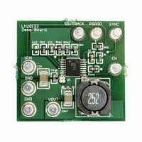
Manufacturer Part Number
LM20133EVAL
Description
BOARD EVAL 3A POWERWISE LM20133
Manufacturer
National Semiconductor
Series
PowerWise®r
Specifications of LM20133EVAL
Main Purpose
DC/DC, Step Down
Outputs And Type
1, Non-Isolated
Voltage - Output
1.2V
Current - Output
3A
Voltage - Input
2.95 ~ 5.5V
Regulator Topology
Buck
Board Type
Fully Populated
Utilized Ic / Part
LM20133
Lead Free Status / RoHS Status
Not applicable / Not applicable
Power - Output
-
Frequency - Switching
-


The power stage transfer function is dictated by the modula-
tor, output LC filter, and load; while the feedback transfer
function is set by the feedback resistor ratio, error amp gain,
and external compensation network.
To achieve a -20dB/decade slope, the error amplifier zero,
located at f
pole (f
can be added to cancel the output filter zero at f
cellation of the output filter zero is recommended if larger
value, non-ceramic output capacitors are used.
Compensation of the LM20133 is achieved by adding an RC
network as shown in Figure 5 below.
A good starting value for C
Once the value of C
calculated using the equation below to cancel the output filter
pole (f
A higher crossover frequency can be obtained, usually at the
expense of phase margin, by lowering the value of C
recalculating the value of R
recalculating R
lower crossover frequency. As with any attempt to compen-
sate the LM20133 the stability of the system should be verified
for desired transient droop and settling time.
If the output filter zero, f
quency (F
at the COMP pin to ground. This capacitor adds a pole to
cancel the output filter zero assuring the crossover frequency
will occur before the double pole at f
margin. The output filter zero is set by the output capacitor
value and ESR as shown in the equation below.
If needed, the value for C
equation shown below.
Where R
R
C1
is the calculated compensation resistance.
FIGURE 5. Compensation Network for LM20133
P(FIL)
P(FIL)
ESR
C
). An additional error amp pole, located at f
) as shown in Figure 4.
Z(EA)
), an additional capacitor (C
is the output capacitor series resistance and
C1
, should positioned to cancel the output filter
will provide additional phase margin at a
C1
is chosen the value of RC should be
Z(FIL)
C2
C1
C1
should be calculated using the
. Likewise, increasing C
approaches the crossover fre-
for most applictions is 4.7 nF.
SW
30030314
/2 degrades the phase
C2
) should be placed
Z(FIL)
C1
C1
. Can-
P2(EA)
and
and
,
15
AVIN FILTERING COMPONENTS (C
To prevent high frequency noise spikes from disturbing the
sensitive analog circuitry connected to the AVIN and AGND
pins, a high frequency RC filter is required between PVIN and
AVIN. These components are shown in Figure 2 as C
R
ommended value of C
should be placed as close to the IC as possible with a direct
connection from AVIN to AGND. A good quality X5R or X7R
ceramic capacitor should be used for C
SUB-REGULATOR BYPASS CAPACITOR (C
The capacitor at the VCC pin provides noise filtering and sta-
bility for the internal sub-regulator. The recommended value
of C
10 µF. The capacitor should be a good quality ceramic X5R
or X7R capacitor. In general, a 1 µF ceramic capacitor is rec-
ommended for most applications.
SETTING THE START UP TIME (C
The addition of a capacitor connected from the SS pin to
ground sets the time at which the output voltage will reach the
final regulated value. Larger values for C
start up times. Table 3, shown below provides a list of soft
start capacitors and the corresponding typical start up times.
If different start up times are needed the equation shown be-
low can be used to calculate the start up time.
As shown above, the start up time is influenced by the value
of the Soft-Start capacitor C
current I
istics table.
While the Soft-Start capacitor can be sized to meet many start
up requirements, there are limitations to its size. The Soft-
Start time can never be faster than 1 ms due to the internal
default 1 ms start up time. When the device is enabled there
is an approximate time interval of 50 µs when the Soft-Start
capacitor will be discharged just prior to the Soft-Start ramp.
If the enable pin is rapidly pulsed or the Soft-Start capacitor
is large there may not be enough time for C
discharge resulting in start up times less than predicted. To
aid in discharging of Soft-Start capacitor during long disable
periods an external 1 MΩ resistor from SS/TRK to ground can
be used without greatly affecting the start-up time.
USING PRECISION ENABLE AND POWER GOOD
The precision enable (EN) and power good (PGOOD) pins of
the LM20133 can be used to address many sequencing re-
quirements. The turn-on of the LM20133 can be controlled
with the precision enable pin by using two external resistors
as shown in Figure 6.
F
. The required value for R
VCC
TABLE 3. Start Up Times for Different Soft-Start
Start Up Time (ms)
should be no smaller than 1 µF and no greater than
SS
(A). that may be found in the electrical character-
10
15
20
1
5
F
Capacitors
is 1.0 µF. The filter capacitor, C
SS
F
(F) and the 5 µA Soft-Start pin
is 1Ω. C
SS
F
)
F
F
and R
SS
.
must be used. Rec-
C
will result in longer
SS
none
100
120
33
68
SS
(nF)
F
)
VCC
to completely
www.national.com
)
F
and
F
Related parts for LM20133EVAL
Image
Part Number
Description
Manufacturer
Datasheet
Request
R

Part Number:
Description:
MODULE TXRX BLUETOOTH 2 18SMD
Manufacturer:
Flexipanel
Datasheet:

Part Number:
Description:
MODULE TXRX BLUETOOTH 2 18DIP
Manufacturer:
Flexipanel
Datasheet:

Part Number:
Description:
LM20 2.4V, 10?A, SC70, micro SMD Temperature Sensor
Manufacturer:
National Semiconductor
Datasheet:
Part Number:
Description:
National Semiconductor [8-Bit D/A Converter]
Manufacturer:
National Semiconductor
Datasheet:
Part Number:
Description:
National Semiconductor [Media Coprocessor]
Manufacturer:
National Semiconductor
Datasheet:
Part Number:
Description:
Digitally Controlled Tone and Volume Circuit with Stereo Audio Power Amplifier, Microphone Preamp Stage and National 3D Sound
Manufacturer:
National Semiconductor
Datasheet:
Part Number:
Description:
Digitally Controlled Tone and Volume Circuit with Stereo Audio Power Amplifier, Microphone Preamp Stage and National 3D Sound
Manufacturer:
National Semiconductor
Datasheet:
Part Number:
Description:
AC97 Rev 2 Codec with Sample Rate Conversion and National 3D Sound
Manufacturer:
National Semiconductor
Part Number:
Description:
Manufacturer:
National Semiconductor
Datasheet:
Part Number:
Description:
Manufacturer:
National Semiconductor
Datasheet:
Part Number:
Description:
General Purpose, Low Voltage, Low Power, Rail-to-Rail Output Operational Amplifiers
Manufacturer:
National Semiconductor
Datasheet:
Part Number:
Description:
8-bit 20 MSPS flash A/D converter.
Manufacturer:
National Semiconductor
Datasheet:
Part Number:
Description:
Low Noise Quad Operational Amplifier
Manufacturer:
National Semiconductor
Datasheet:
Part Number:
Description:
Quad Differential Line Receivers
Manufacturer:
National Semiconductor
Datasheet: