LM2653-ADJEVAL National Semiconductor, LM2653-ADJEVAL Datasheet - Page 9
LM2653-ADJEVAL
Manufacturer Part Number
LM2653-ADJEVAL
Description
EVALUATION BOARD FOR LM2653-ADJ
Manufacturer
National Semiconductor
Specifications of LM2653-ADJEVAL
Main Purpose
DC/DC, Step Down
Outputs And Type
1, Non-Isolated
Voltage - Output
2.5V
Current - Output
1.5A
Voltage - Input
4 ~ 14V
Regulator Topology
Buck
Frequency - Switching
300kHz
Board Type
Fully Populated
Utilized Ic / Part
LM2653
Lead Free Status / RoHS Status
Lead free / RoHS Compliant
Power - Output
-
Other names
*LM2653-ADJEVAL


Design Procedure
R
Use the following formula to select the appropriate resistor
values:
where V
Select resistors between 10kΩ and 100kΩ. (1% or higher
accuracy metal film resistors for R
COMPENSATION COMPONENTS
In the control to output transfer function, the first pole F
be estimated as 1/(2πR
output capacitor is 1/(2πESRC
frequency pole F
where D = V
and V
The total loop gain G is approximately 500/I
is in amperes.
A Gm amplifier is used inside the LM2653. The output resis-
tor R
together with R
In some applications, the ESR zero F
by F
ESR zero, F
The rule of thumb is to have more than 45˚ phase margin at
the crossover frequency (G=1).
If C
good choices for most applications. If the ESR zero is too
low to be cancelled by F
If the transient response to a step load is important, choose
R
EXTERNAL SCHOTTKY DIODE
A Schottky diode D
body diode of the low-side MOSFET from conducting during
1
C
and R
OUT
to be higher than 10kΩ.
p2
o
IN
. Then, C
of the Gm amplifier is about 80kΩ. C
is higher than 68µF, C
F
REF
and V
pc1
2
(PROGRAMMING OUTPUT VOLTAGE)
p2
= 1.238V
OUT
= 1/(2πC
OUT
o
= 1/(2πC
c2
/V
give a lag compensation to roll off the gain:
p2
V
is needed to introduce F
IN
1
in volts).
OUT
in the range of 45kHz to 150kHz:
F
, n = 1+0.348L/(V
is recommended to prevent the intrinsic
p2
c1
= V
OUT
(R
c2
= F
p2
R
o
, add C
+R
REF
C
o
s
\R
/(πn(1−D))
OUT
c1
c
(1 + R
)), F
c
).
OUT
= 2.2nF, and R
); The ESR zero F
(Continued)
c2
1
zc1
); Also, there is a high
.
and R
z1
1
/R
IN
= 1/2πC
can not be cancelled
−V
2
)
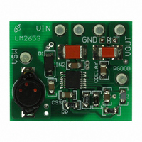
Schematic for the Typical Board Layout
2
OUT
pc2
.)
OUT
) (L is in µHs
c1
to cancel the
c
= 15KΩ are
where I
R
c1
c
.
z1
and R
p1
of the
can
OUT
C
9
the deadtime in PWM operation and hysteretic mode when
both MOSFETs are off. If the body diode turns on, there is
extra power dissipation in the body diode because of the
reverse-recovery current and higher forward voltage; the
high-side MOSFET also has more switching loss since the
negative diode reverse-recovery current appears as the
high-side MOSFET turn-on current in addition to the load
current. These losses degrade the efficiency by 1-2%. The
improved efficiency and noise immunity with the Schottky
diode become more obvious with increasing input voltage
and load current.
The breakdown voltage rating of D
higher than the maximum input voltage. Since D
for a short period of time, the average current rating for D
only requires being higher than 30% of the maximum output
current. It is important to place D
source of the low-side MOSFET, extra parasitic inductance
in the parallel loop will slow the turn-on of D
current through the body diode of the low-side MOSFET.
PCB Layout Considerations
Layout is critical to reduce noises and ensure specified
performance. The important guidelines are listed as follows:
1. Minimize the parasitic inductance in the loop of input
2. Minimize the trace from the center of the output resistor
3. If the Schottky diode D
capacitors and the internal MOSFETs by connecting the
input capacitors to V
wide traces. This is important because the rapidly
switching current, together with wiring inductance can
generate large voltage spikes that may result in noise
problems.
divider to the FB pin and keep it away from noise
sources to avoid noise pick up. For applications require
tight regulation at the output, a dedicated sense trace
(separated from the power trace) is recommended to
connect the top of the resistor divider to the output.
connecting D
1
to SW and PGND pins.
IN
and PGND pins with short and
1
is used, minimize the traces
10104901
1
very close to the drain and
1
is preferred to be 25%
1
and direct the
1
www.national.com
is only on
1
Related parts for LM2653-ADJEVAL
Image
Part Number
Description
Manufacturer
Datasheet
Request
R

Part Number:
Description:
National Semiconductor [8-Bit D/A Converter]
Manufacturer:
National Semiconductor
Datasheet:
Part Number:
Description:
National Semiconductor [Media Coprocessor]
Manufacturer:
National Semiconductor
Datasheet:
Part Number:
Description:
Digitally Controlled Tone and Volume Circuit with Stereo Audio Power Amplifier, Microphone Preamp Stage and National 3D Sound
Manufacturer:
National Semiconductor
Datasheet:
Part Number:
Description:
Digitally Controlled Tone and Volume Circuit with Stereo Audio Power Amplifier, Microphone Preamp Stage and National 3D Sound
Manufacturer:
National Semiconductor
Datasheet:
Part Number:
Description:
AC97 Rev 2 Codec with Sample Rate Conversion and National 3D Sound
Manufacturer:
National Semiconductor
Part Number:
Description:
Manufacturer:
National Semiconductor
Datasheet:
Part Number:
Description:
Manufacturer:
National Semiconductor
Datasheet:
Part Number:
Description:
General Purpose, Low Voltage, Low Power, Rail-to-Rail Output Operational Amplifiers
Manufacturer:
National Semiconductor
Datasheet:
Part Number:
Description:
8-bit 20 MSPS flash A/D converter.
Manufacturer:
National Semiconductor
Datasheet:
Part Number:
Description:
Low Noise Quad Operational Amplifier
Manufacturer:
National Semiconductor
Datasheet:
Part Number:
Description:
Quad Differential Line Receivers
Manufacturer:
National Semiconductor
Datasheet:
Part Number:
Description:
Quad High Speed Trapezoidal? Bus Transceiver
Manufacturer:
National Semiconductor
Datasheet:
Part Number:
Description:
Dual Line Receiver
Manufacturer:
National Semiconductor
Datasheet:
Part Number:
Description:
TTL to 10k ECL Level Translator with Latch
Manufacturer:
National Semiconductor
Datasheet: