NCP1052GEVB ON Semiconductor, NCP1052GEVB Datasheet - Page 6
NCP1052GEVB
Manufacturer Part Number
NCP1052GEVB
Description
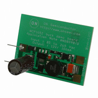
EVAL BOARD FOR NCP1052G
Manufacturer
ON Semiconductor
Specifications of NCP1052GEVB
Design Resources
NCP1052 Eval Board BOM NCP1052GEVB Gerber Files NCP1052 Demo Board Schematic
Main Purpose
AC/DC, Non-Isolated
Outputs And Type
1, Non-Isolated
Power - Output
1.2W
Voltage - Output
120V
Current - Output
100mA
Voltage - Input
85 ~ 265VAC
Regulator Topology
Boost, Buck
Frequency - Switching
136kHz
Board Type
Fully Populated
Utilized Ic / Part
NCP1052
Lead Free Status / RoHS Status
Lead free / RoHS Compliant
For Use With/related Products
NCP1052G
Other names
NCP1052GEVBOS


ability. It is because the V
only passes through the inductor. The charging current
pulses become an averaged energy stored in the inductor and
consume smaller amount of power comparing to the buck
case.
7 is a method to improve the standby ability. The auxiliary
winding keeps the V
V
auxiliary winding is coupled from the inductor L with
polarity same as the regulated output voltage. The V
voltage in the auxiliary winding is designed to be between
the normal V
frequency jittering feature loses when the V
fixed. When output is shorted, there will be no voltage
coming from the auxiliary winding and the circuit will enter
CC
The proposed buck-boost is better in term of the standby
The auxiliary winding to supply the V
Figure 7. Auxiliary Winding to improve standby
charging current and hence its standby loss. The
CC
limits of 7.5 and 8.5 V typically. The
CC
(b) Buck-boost
voltage above 7.5 V and disable the
(a) Buck
CC
Abillity
charging current in Figure 2(b)
CC
voltage in Figure
CC
voltage is
http://onsemi.com
AND8098/D
CC
6
fault mode with the 4.5 V-8.5 V-7.5 V-4.5 V hysteresis
loop.
capacitor technique in Figure 8. The output voltage is
coupled to the inserted capacitor when the diodes are closed.
The voltage drop of the diodes compensate each other.
Hence, the diode voltage drop effect can be neglected. The
NCP1052 needs a nominal V
resistor consumes some voltage from the output voltage V
to make a 8V to the V
current consumption of V
value is (V
Temperature Rise
circuit and high-voltage power switch. Its typical on
resistance is 22
recommended to design the PCB board with a large copper
area next to the device as a heatsink. This heatsink decreases
Another method to supply the V
The NCP1052 is a very compact package with the control
Figure 8. Coupling Capacitor Technique to
out
- 8) / 0.5 kW.
Improve Standby Abillity
(b) Buck-boost
. Temperature rise exists. It is
CC
(a) Buck
pin. Based on the 0.5mA typical
CC
CC
pin. The inserted resistance
voltage of 8V. The inserted
CC
voltage is coupling
out
Related parts for NCP1052GEVB
Image
Part Number
Description
Manufacturer
Datasheet
Request
R

Part Number:
Description:
ON Semiconductor [VOLTAGE REGULATOR]
Manufacturer:
ON Semiconductor
Datasheet:
Part Number:
Description:
357-036-542-201 CARDEDGE 36POS DL .156 BLK LOPRO
Manufacturer:
ON Semiconductor
Datasheet:
Part Number:
Description:
357-036-542-201 CARDEDGE 36POS DL .156 BLK LOPRO
Manufacturer:
ON Semiconductor
Datasheet:
Part Number:
Description:
357-036-542-201 CARDEDGE 36POS DL .156 BLK LOPRO
Manufacturer:
ON Semiconductor
Datasheet:
Part Number:
Description:
357-036-542-201 CARDEDGE 36POS DL .156 BLK LOPRO
Manufacturer:
ON Semiconductor
Datasheet:
Part Number:
Description:
357-036-542-201 CARDEDGE 36POS DL .156 BLK LOPRO
Manufacturer:
ON Semiconductor
Datasheet:
Part Number:
Description:
357-036-542-201 CARDEDGE 36POS DL .156 BLK LOPRO
Manufacturer:
ON Semiconductor
Datasheet:
Part Number:
Description:
357-036-542-201 CARDEDGE 36POS DL .156 BLK LOPRO
Manufacturer:
ON Semiconductor
Datasheet:
Part Number:
Description:
357-036-542-201 CARDEDGE 36POS DL .156 BLK LOPRO
Manufacturer:
ON Semiconductor
Datasheet:
Part Number:
Description:
357-036-542-201 CARDEDGE 36POS DL .156 BLK LOPRO
Manufacturer:
ON Semiconductor
Datasheet:
Part Number:
Description:
357-036-542-201 CARDEDGE 36POS DL .156 BLK LOPRO
Manufacturer:
ON Semiconductor
Datasheet:
Part Number:
Description:
Manufacturer:
ON Semiconductor
Datasheet:
Part Number:
Description:
Manufacturer:
ON Semiconductor
Datasheet:
Part Number:
Description:
Manufacturer:
ON Semiconductor
Datasheet: