NCP1421EVB ON Semiconductor, NCP1421EVB Datasheet - Page 13
NCP1421EVB
Manufacturer Part Number
NCP1421EVB
Description
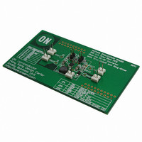
EVAL BOARD FOR NCP1421
Manufacturer
ON Semiconductor
Specifications of NCP1421EVB
Design Resources
NCP1421 Demo Board BOM NCP1421EVB Gerber Files NCP1421 Demo Board Schematic
Main Purpose
DC/DC, Step Up
Outputs And Type
1, Non-Isolated
Voltage - Output
3.3V or 5V
Current - Output
600mA
Voltage - Input
3V
Regulator Topology
Boost
Frequency - Switching
1.2MHz
Board Type
Fully Populated
Utilized Ic / Part
NCP1421
Lead Free Status / RoHS Status
Lead free / RoHS Compliant
Power - Output
-
Lead Free Status / Rohs Status
Lead free / RoHS Compliant
For Use With/related Products
NCP1421
Other names
NCP1421EVBOS


−T−
0.038 (0.0015)
SEATING
PLANE
PIN 1 ID
K
G
−A−
*For additional information on our Pb−Free strategy and soldering
H
details, please download the ON Semiconductor Soldering and
Mounting Techniques Reference Manual, SOLDERRM/D.
C
D
−B−
8X
8 PL
0.041
0.08 (0.003)
1.04
6X
0.0256
0.65
0.126
J
3.20
PACKAGE DIMENSIONS
SOLDERING FOOTPRINT*
M
http://onsemi.com
CASE 846A−02
T
DM SUFFIX
NCP1421
B
ISSUE F
Micro8
S
13
A
0.015
0.38
L
S
8X
0.167
SCALE 8:1
4.24
0.208
5.28
inches
mm
NOTES:
1. DIMENSIONING AND TOLERANCING PER ANSI
2. CONTROLLING DIMENSION: MILLIMETER.
3. DIMENSION A DOES NOT INCLUDE MOLD
4. DIMENSION B DOES NOT INCLUDE INTERLEAD
5. 846A−01 OBSOLETE, NEW STANDARD 846A−02.
Y14.5M, 1982.
FLASH, PROTRUSIONS OR GATE BURRS. MOLD
FLASH, PROTRUSIONS OR GATE BURRS SHALL
NOT EXCEED 0.15 (0.006) PER SIDE.
FLASH OR PROTRUSION. INTERLEAD FLASH OR
PROTRUSION SHALL NOT EXCEED 0.25 (0.010)
PER SIDE.
DIM
A
B
C
D
G
H
K
J
L
MILLIMETERS
MIN
2.90
2.90
0.25
0.05
0.13
4.75
0.40
−−−
0.65 BSC
MAX
3.10
3.10
1.10
0.40
0.15
0.23
5.05
0.70
0.010
0.002
0.005
0.187
0.016
0.114
0.114
MIN
−−−
0.026 BSC
INCHES
MAX
0.122
0.122
0.043
0.016
0.006
0.009
0.199
0.028
Related parts for NCP1421EVB
Image
Part Number
Description
Manufacturer
Datasheet
Request
R

Part Number:
Description:
600 Ma Sync-rect Pfm Step-up Dc-dc Converter Step-up Dc-dc Converter With True-cutoff And Ring-killer
Manufacturer:
ON Semiconductor
Datasheet:
Part Number:
Description:
ON Semiconductor [VOLTAGE REGULATOR]
Manufacturer:
ON Semiconductor
Datasheet:
Part Number:
Description:
357-036-542-201 CARDEDGE 36POS DL .156 BLK LOPRO
Manufacturer:
ON Semiconductor
Datasheet:
Part Number:
Description:
357-036-542-201 CARDEDGE 36POS DL .156 BLK LOPRO
Manufacturer:
ON Semiconductor
Datasheet:
Part Number:
Description:
357-036-542-201 CARDEDGE 36POS DL .156 BLK LOPRO
Manufacturer:
ON Semiconductor
Datasheet:
Part Number:
Description:
357-036-542-201 CARDEDGE 36POS DL .156 BLK LOPRO
Manufacturer:
ON Semiconductor
Datasheet:
Part Number:
Description:
357-036-542-201 CARDEDGE 36POS DL .156 BLK LOPRO
Manufacturer:
ON Semiconductor
Datasheet:
Part Number:
Description:
357-036-542-201 CARDEDGE 36POS DL .156 BLK LOPRO
Manufacturer:
ON Semiconductor
Datasheet:
Part Number:
Description:
357-036-542-201 CARDEDGE 36POS DL .156 BLK LOPRO
Manufacturer:
ON Semiconductor
Datasheet:
Part Number:
Description:
357-036-542-201 CARDEDGE 36POS DL .156 BLK LOPRO
Manufacturer:
ON Semiconductor
Datasheet:
Part Number:
Description:
357-036-542-201 CARDEDGE 36POS DL .156 BLK LOPRO
Manufacturer:
ON Semiconductor
Datasheet:
Part Number:
Description:
357-036-542-201 CARDEDGE 36POS DL .156 BLK LOPRO
Manufacturer:
ON Semiconductor
Datasheet:
Part Number:
Description:
Manufacturer:
ON Semiconductor
Datasheet:
Part Number:
Description:
Manufacturer:
ON Semiconductor
Datasheet: