NCP1421EVB ON Semiconductor, NCP1421EVB Datasheet - Page 7
NCP1421EVB
Manufacturer Part Number
NCP1421EVB
Description
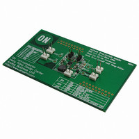
EVAL BOARD FOR NCP1421
Manufacturer
ON Semiconductor
Specifications of NCP1421EVB
Design Resources
NCP1421 Demo Board BOM NCP1421EVB Gerber Files NCP1421 Demo Board Schematic
Main Purpose
DC/DC, Step Up
Outputs And Type
1, Non-Isolated
Voltage - Output
3.3V or 5V
Current - Output
600mA
Voltage - Input
3V
Regulator Topology
Boost
Frequency - Switching
1.2MHz
Board Type
Fully Populated
Utilized Ic / Part
NCP1421
Lead Free Status / RoHS Status
Lead free / RoHS Compliant
Power - Output
-
Lead Free Status / Rohs Status
Lead free / RoHS Compliant
For Use With/related Products
NCP1421
Other names
NCP1421EVBOS


12.5
−10
7.5
5.0
2.5
10
−5
50
40
30
20
10
15
10
5
0
0
10
1.5
1.5
Figure 16. Battery Input Voltage vs. Output Ripple
Figure 18. No Load Operating Current vs. Input
Figure 14. Output Voltage Change vs. Load
V
L = 5.6 mH
C
C
T
A
OUT
IN
OUT
V
V
L = 6.8 mH
C
C
T
= 25_C
A
IN
OUT
IN
OUT
= 22 mF
2.0
= 25_C
= 2.5 V
= 22 mF
= 3.3 V
= 22 mF
OUTPUT LOADING CURRENT, I
1.7
INPUT VOLTAGE AT OUT PIN, V
= 3.3 V
= 22 mF
BATTERY INPUT VOLTAGE, V
2.5
Voltage at OUT Pin
1.9
3.0
Current
Voltage
100
3.5
500 mA
300 mA
100 mA
TYPICAL OPERATING CHARACTERISTICS
2.1
4.0
LOAD
BATT
OUT
V
V
2.3
IN
IN
/V
/mA
/V
= 2.5 V
= 2.0 V
4.5
http://onsemi.com
1000
NCP1421
2.5
5.0
7
−10
10
−5
5
0
10
Upper Trace: Voltage at LBI Pin, 1.0 V/Division
Lower Trace: Voltage at LBO Pin, 1.0 V/Division
Upper Trace: Input Voltage Waveform, 1.0 V/Division
Lower Trace: Output Voltage Waveform, 2.0 V/Division
V
L = 5.6 mH
C
C
T
A
OUT
IN
OUT
Figure 15. Output Voltage Change vs. Load
= 25_C
= 22 mF
Figure 19. Startup Transient Response
= 5.0 V
= 22 mF
OUTPUT LOADING CURRENT, I
Figure 17. Low Battery Detect
Current
100
V
IN
= 1.5 V
V
V
I
LOAD
IN
OUT
LOAD
= 2.5 V
V
= 5.0 V
= 10 mA
IN
V
IN
/mA
= 2.5 V
= 3.3 V
1000
Related parts for NCP1421EVB
Image
Part Number
Description
Manufacturer
Datasheet
Request
R

Part Number:
Description:
600 Ma Sync-rect Pfm Step-up Dc-dc Converter Step-up Dc-dc Converter With True-cutoff And Ring-killer
Manufacturer:
ON Semiconductor
Datasheet:
Part Number:
Description:
ON Semiconductor [VOLTAGE REGULATOR]
Manufacturer:
ON Semiconductor
Datasheet:
Part Number:
Description:
357-036-542-201 CARDEDGE 36POS DL .156 BLK LOPRO
Manufacturer:
ON Semiconductor
Datasheet:
Part Number:
Description:
357-036-542-201 CARDEDGE 36POS DL .156 BLK LOPRO
Manufacturer:
ON Semiconductor
Datasheet:
Part Number:
Description:
357-036-542-201 CARDEDGE 36POS DL .156 BLK LOPRO
Manufacturer:
ON Semiconductor
Datasheet:
Part Number:
Description:
357-036-542-201 CARDEDGE 36POS DL .156 BLK LOPRO
Manufacturer:
ON Semiconductor
Datasheet:
Part Number:
Description:
357-036-542-201 CARDEDGE 36POS DL .156 BLK LOPRO
Manufacturer:
ON Semiconductor
Datasheet:
Part Number:
Description:
357-036-542-201 CARDEDGE 36POS DL .156 BLK LOPRO
Manufacturer:
ON Semiconductor
Datasheet:
Part Number:
Description:
357-036-542-201 CARDEDGE 36POS DL .156 BLK LOPRO
Manufacturer:
ON Semiconductor
Datasheet:
Part Number:
Description:
357-036-542-201 CARDEDGE 36POS DL .156 BLK LOPRO
Manufacturer:
ON Semiconductor
Datasheet:
Part Number:
Description:
357-036-542-201 CARDEDGE 36POS DL .156 BLK LOPRO
Manufacturer:
ON Semiconductor
Datasheet:
Part Number:
Description:
357-036-542-201 CARDEDGE 36POS DL .156 BLK LOPRO
Manufacturer:
ON Semiconductor
Datasheet:
Part Number:
Description:
Manufacturer:
ON Semiconductor
Datasheet:
Part Number:
Description:
Manufacturer:
ON Semiconductor
Datasheet: