NCP1422EVB ON Semiconductor, NCP1422EVB Datasheet
NCP1422EVB
Manufacturer Part Number
NCP1422EVB
Description
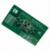
EVAL BOARD FOR NCP1422
Manufacturer
ON Semiconductor
Specifications of NCP1422EVB
Design Resources
NCP1422 EVB BOM NCP1422EVB Gerber Files NCP1422EVB Schematic
Main Purpose
DC/DC, Step Up
Outputs And Type
1, Non-Isolated
Voltage - Output
3.3 ~ 5 V
Current - Output
800mA
Voltage - Input
2.5V, 3.6V
Regulator Topology
Boost
Frequency - Switching
1.2MHz
Board Type
Fully Populated
Utilized Ic / Part
NCP1422
Lead Free Status / RoHS Status
Lead free / RoHS Compliant
Power - Output
-
Lead Free Status / Rohs Status
Lead free / RoHS Compliant
For Use With/related Products
NCP1422
Other names
NCP1422EVBOS
12/13/2007
1. Connect the test setup as shown above.
2. TURN OFF the JP; (enable the device).
3. Set the Power Supply to 3.0V and apply to TP1, TP2, (T1, T2).
4. Apply 500mA loading form the electric load.
5. Check the input current (I
6. Check the switching waveform at scope CH1 to see whether it is a normal
continuous conduction mode switching node waveform and switching ON time
(T
ON
• For V
• For V
) is between 0.46 µs ~ 1.15 µs
Test Procedure for the NCP1422 Evaluation Board
I
V
V
I
V
V
IN
IN
OUT
RIPPLE
OUT
RIPPLE
= 590.7mA ~ 608.7mA
= 931.07mA ~ 957.4mA
= 3.267 ~ 3.367V
= 4.859 ~ 5.0075V
OUT
OUT
≤ 35mV
≤ 40mV
= 3.3V; JP2 OFF
= 5V; JP2 ON
IN
), output voltage (V
- 1 -
OUT
) and output ripple;
www.onsemi.com
Related parts for NCP1422EVB
Image
Part Number
Description
Manufacturer
Datasheet
Request
R

Part Number:
Description:
Sync-Rect PFM Step-Up DC-DC Converter
Manufacturer:
ON Semiconductor
Datasheet:
Part Number:
Description:
ON Semiconductor [VOLTAGE REGULATOR]
Manufacturer:
ON Semiconductor
Datasheet:
Part Number:
Description:
357-036-542-201 CARDEDGE 36POS DL .156 BLK LOPRO
Manufacturer:
ON Semiconductor
Datasheet:
Part Number:
Description:
357-036-542-201 CARDEDGE 36POS DL .156 BLK LOPRO
Manufacturer:
ON Semiconductor
Datasheet:
Part Number:
Description:
357-036-542-201 CARDEDGE 36POS DL .156 BLK LOPRO
Manufacturer:
ON Semiconductor
Datasheet:
Part Number:
Description:
357-036-542-201 CARDEDGE 36POS DL .156 BLK LOPRO
Manufacturer:
ON Semiconductor
Datasheet:
Part Number:
Description:
357-036-542-201 CARDEDGE 36POS DL .156 BLK LOPRO
Manufacturer:
ON Semiconductor
Datasheet:
Part Number:
Description:
357-036-542-201 CARDEDGE 36POS DL .156 BLK LOPRO
Manufacturer:
ON Semiconductor
Datasheet:
Part Number:
Description:
357-036-542-201 CARDEDGE 36POS DL .156 BLK LOPRO
Manufacturer:
ON Semiconductor
Datasheet:
Part Number:
Description:
357-036-542-201 CARDEDGE 36POS DL .156 BLK LOPRO
Manufacturer:
ON Semiconductor
Datasheet:
Part Number:
Description:
357-036-542-201 CARDEDGE 36POS DL .156 BLK LOPRO
Manufacturer:
ON Semiconductor
Datasheet:
Part Number:
Description:
357-036-542-201 CARDEDGE 36POS DL .156 BLK LOPRO
Manufacturer:
ON Semiconductor
Datasheet:
Part Number:
Description:
Manufacturer:
ON Semiconductor
Datasheet:
Part Number:
Description:
Manufacturer:
ON Semiconductor
Datasheet: