LM2595ADPBCKGEVB ON Semiconductor, LM2595ADPBCKGEVB Datasheet - Page 18
LM2595ADPBCKGEVB
Manufacturer Part Number
LM2595ADPBCKGEVB
Description
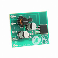
EVAL BOARD FOR LM2595ADPBCKG
Manufacturer
ON Semiconductor
Specifications of LM2595ADPBCKGEVB
Design Resources
LM2595ADPBCKGEVB BOM LM2595ADPBCKGEVB Gerber Files LM2595ADPBCKGEVB Schematic
Main Purpose
DC/DC, Step Down
Outputs And Type
1, Non-Isolated
Voltage - Output
5V
Current - Output
1A
Voltage - Input
4.5 ~ 40 V
Regulator Topology
Buck
Frequency - Switching
150kHz
Board Type
Fully Populated
Utilized Ic / Part
LM2595
Lead Free Status / RoHS Status
Lead free / RoHS Compliant
Power - Output
-
Lead Free Status / Rohs Status
Lead free / RoHS Compliant
For Use With/related Products
LM2595ADPBCKG
Other names
LM2595ADPBCKGEVBOS


ADDITIONAL APPLICATIONS
Inverting Regulator
shown in Figure 23. This circuit converts a positive input
voltage to a negative output voltage with a common ground
by bootstrapping the regulators ground to the negative
output voltage. By grounding the feedback pin, the regulator
senses the inverted output voltage and regulates it.
output. The maximum input voltage in this case cannot
exceed +28 V because the maximum voltage appearing
across the regulator is the absolute sum of the input and
output voltages and this must be limited to a maximum of
40 V.
0.25 A to the output when the input voltage is 12 V or higher.
At lighter loads the minimum input voltage required drops
to approximately 4.7 V, because the buck−boost regulator
topology can produce an output voltage that, in its absolute
value, is either greater or less than the input voltage.
are higher than in the standard buck converter topology, the
available output current is lower.
require a larger amount of startup input current, even for
light loads. This may overload an input power source with
a current limit less than 1.0 A.
least 2.0 ms or more. The actual time depends on the output
voltage and size of the output capacitor.
this inverting regulator topology, the use of a delayed startup
or an undervoltage lockout circuit is recommended.
An inverting buck−boost regulator using the LM2595 is
In this example the LM2595 is used to generate a −12 V
This circuit configuration is able to deliver approximately
Since the switch currents in this buck−boost configuration
This type of buck−boost inverting regulator can also
Such an amount of input startup current is needed for at
Because of the relatively high startup currents required by
100 mF/50 V
Unregulated
12 to 40 V
DC Input
C
in
Figure 24. Inverting Buck−Boost Develops with Delayed Startup
0.1 mF
C1
+V
in
ON/OFF
R2
47k
LM2595
http://onsemi.com
GND
18
Feedback
can charge up to a higher voltage before the switch−mode
regulator begins to operate.
supplied by the input capacitor C
situations, the delayed startup or the undervoltage lockout
features could be very useful. A delayed startup circuit
applied to a buck−boost converter is shown in Figure 28.
Figure 30 in the “Undervoltage Lockout” section describes
an undervoltage lockout feature for the same converter
topology.
Design Recommendations:
than the buck converter and so a different design procedure
has to be used to select the inductor L1 or the output
capacitor C
normally required for buck converter designs. Low input
voltages or high output currents require a large value output
capacitor (in the range of thousands of mF).
inverting converter design is between 68 mH and 220 mH. To
select an inductor with an appropriate current rating, the
inductor peak current has to be calculated.
current:
conditions, the worst case occurs when V
where t on +
Using a delayed startup arrangement, the input capacitor
The high input current needed for startup is now partially
It has been already mentioned above, that in some
The inverting regulator operates in a different manner
The output capacitor values must be larger than what is
The recommended range of inductor values for the
The following formula is used to obtain the peak inductor
Under normal continuous inductor current operating
D1
1N5819
100 mH
L1
I
peak
out
.
[
C
220 mF
V
out
in
I
R3
Load
|V
) |V
O
|
(V
O
V
in
|
in
x 1.0
C
−12 V @ 0.25 A
) |V
R4
FF
f osc
Regulated
in
Output
.
O
, and f osc + 52 kHz.
|)
)
in
V
is minimal.
in
2L 1
x t on
Related parts for LM2595ADPBCKGEVB
Image
Part Number
Description
Manufacturer
Datasheet
Request
R

Part Number:
Description:
ON Semiconductor [VOLTAGE REGULATOR]
Manufacturer:
ON Semiconductor
Datasheet:
Part Number:
Description:
357-036-542-201 CARDEDGE 36POS DL .156 BLK LOPRO
Manufacturer:
ON Semiconductor
Datasheet:
Part Number:
Description:
357-036-542-201 CARDEDGE 36POS DL .156 BLK LOPRO
Manufacturer:
ON Semiconductor
Datasheet:
Part Number:
Description:
357-036-542-201 CARDEDGE 36POS DL .156 BLK LOPRO
Manufacturer:
ON Semiconductor
Datasheet:
Part Number:
Description:
357-036-542-201 CARDEDGE 36POS DL .156 BLK LOPRO
Manufacturer:
ON Semiconductor
Datasheet:
Part Number:
Description:
357-036-542-201 CARDEDGE 36POS DL .156 BLK LOPRO
Manufacturer:
ON Semiconductor
Datasheet:
Part Number:
Description:
357-036-542-201 CARDEDGE 36POS DL .156 BLK LOPRO
Manufacturer:
ON Semiconductor
Datasheet:
Part Number:
Description:
357-036-542-201 CARDEDGE 36POS DL .156 BLK LOPRO
Manufacturer:
ON Semiconductor
Datasheet:
Part Number:
Description:
357-036-542-201 CARDEDGE 36POS DL .156 BLK LOPRO
Manufacturer:
ON Semiconductor
Datasheet:
Part Number:
Description:
357-036-542-201 CARDEDGE 36POS DL .156 BLK LOPRO
Manufacturer:
ON Semiconductor
Datasheet:
Part Number:
Description:
357-036-542-201 CARDEDGE 36POS DL .156 BLK LOPRO
Manufacturer:
ON Semiconductor
Datasheet:
Part Number:
Description:
Manufacturer:
ON Semiconductor
Datasheet:
Part Number:
Description:
Manufacturer:
ON Semiconductor
Datasheet:
Part Number:
Description:
Manufacturer:
ON Semiconductor
Datasheet: