LM2595ADPBCKGEVB ON Semiconductor, LM2595ADPBCKGEVB Datasheet - Page 5
LM2595ADPBCKGEVB
Manufacturer Part Number
LM2595ADPBCKGEVB
Description
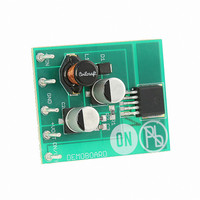
EVAL BOARD FOR LM2595ADPBCKG
Manufacturer
ON Semiconductor
Specifications of LM2595ADPBCKGEVB
Design Resources
LM2595ADPBCKGEVB BOM LM2595ADPBCKGEVB Gerber Files LM2595ADPBCKGEVB Schematic
Main Purpose
DC/DC, Step Down
Outputs And Type
1, Non-Isolated
Voltage - Output
5V
Current - Output
1A
Voltage - Input
4.5 ~ 40 V
Regulator Topology
Buck
Frequency - Switching
150kHz
Board Type
Fully Populated
Utilized Ic / Part
LM2595
Lead Free Status / RoHS Status
Lead free / RoHS Compliant
Power - Output
-
Lead Free Status / Rohs Status
Lead free / RoHS Compliant
For Use With/related Products
LM2595ADPBCKG
Other names
LM2595ADPBCKGEVBOS


−0.5
-0.2
-0.4
-0.6
-0.8
-1.0
1.5
1.0
0.5
12
10
1.0
0.8
0.6
0.4
0.2
11
−50
0
9
8
7
6
5
4
0
0
−50
V
I
Normalized at T
Load
−25
in
−25
5
Figure 3. Normalized Output Voltage
= 20 V
= 200 mA
T
T
J
J
Figure 7. Quiescent Current
, JUNCTION TEMPERATURE (°C)
, JUNCTION TEMPERATURE (°C)
10
Figure 5. Dropout Voltage
I
Load
I
0
Load
0
V
in
I
Load
TYPICAL PERFORMANCE CHARACTERISTICS
= 200 mA
, INPUT VOLTAGE (V)
J
= 1 A
15
= 25°C
25
= 200 mA
25
20
I
V
Measured at GND Pin
T
Load
50
60
out
J
= 25°C
25
= 5 V
= 1.0 A
L = 68 mH
R_ind = 30 mW
75
75
30
100
100
35
http://onsemi.com
125
125
40
5
−0.2
−0.4
−0.6
160
140
120
100
1.4
1.2
1.0
0.8
0.6
0.4
0.2
3.0
2.0
1.0
0.0
80
60
40
20
−50
0
0
−50 −30 −10
0
V
I
T
Load
ON/OFF
J
−25
= 25°C
5.0
Figure 8. Standby Quiescent Current
= 200 mA
T
V
T
= 5.0 V
(Circuit of Figure 16)
J
out
J
, JUNCTION TEMPERATURE (°C)
, JUNCTION TEMPERATURE (°C)
Figure 4. Line Regulation
10
Figure 6. Current Limit
= 5 V
0
V
10
in
, INPUT VOLTAGE (V)
V
V
15
in
in
30
= 40 V
= 12 V
25
20
50
60
70
25
75
90
30
V
in
110
= 12 V
100
35
130
125
40
Related parts for LM2595ADPBCKGEVB
Image
Part Number
Description
Manufacturer
Datasheet
Request
R

Part Number:
Description:
ON Semiconductor [VOLTAGE REGULATOR]
Manufacturer:
ON Semiconductor
Datasheet:
Part Number:
Description:
357-036-542-201 CARDEDGE 36POS DL .156 BLK LOPRO
Manufacturer:
ON Semiconductor
Datasheet:
Part Number:
Description:
357-036-542-201 CARDEDGE 36POS DL .156 BLK LOPRO
Manufacturer:
ON Semiconductor
Datasheet:
Part Number:
Description:
357-036-542-201 CARDEDGE 36POS DL .156 BLK LOPRO
Manufacturer:
ON Semiconductor
Datasheet:
Part Number:
Description:
357-036-542-201 CARDEDGE 36POS DL .156 BLK LOPRO
Manufacturer:
ON Semiconductor
Datasheet:
Part Number:
Description:
357-036-542-201 CARDEDGE 36POS DL .156 BLK LOPRO
Manufacturer:
ON Semiconductor
Datasheet:
Part Number:
Description:
357-036-542-201 CARDEDGE 36POS DL .156 BLK LOPRO
Manufacturer:
ON Semiconductor
Datasheet:
Part Number:
Description:
357-036-542-201 CARDEDGE 36POS DL .156 BLK LOPRO
Manufacturer:
ON Semiconductor
Datasheet:
Part Number:
Description:
357-036-542-201 CARDEDGE 36POS DL .156 BLK LOPRO
Manufacturer:
ON Semiconductor
Datasheet:
Part Number:
Description:
357-036-542-201 CARDEDGE 36POS DL .156 BLK LOPRO
Manufacturer:
ON Semiconductor
Datasheet:
Part Number:
Description:
357-036-542-201 CARDEDGE 36POS DL .156 BLK LOPRO
Manufacturer:
ON Semiconductor
Datasheet:
Part Number:
Description:
Manufacturer:
ON Semiconductor
Datasheet:
Part Number:
Description:
Manufacturer:
ON Semiconductor
Datasheet:
Part Number:
Description:
Manufacturer:
ON Semiconductor
Datasheet: