MCP4725DM-PTPLS Microchip Technology, MCP4725DM-PTPLS Datasheet - Page 16
MCP4725DM-PTPLS
Manufacturer Part Number
MCP4725DM-PTPLS
Description
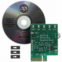
BOARD DAUGHTER PICTAIL MCP4725
Manufacturer
Microchip Technology
Specifications of MCP4725DM-PTPLS
Number Of Dac's
1
Number Of Bits
12
Outputs And Type
1, Single Ended
Sampling Rate (per Second)
100k ~ 3.4M
Data Interface
I²C
Settling Time
6µs
Dac Type
Voltage
Voltage Supply Source
Single
Operating Temperature
-40°C ~ 125°C
Utilized Ic / Part
MCP4725
Silicon Manufacturer
Microchip
Application Sub Type
DAC
Kit Application Type
Data Converter
Silicon Core Number
MCP4725
Silicon Family Name
PICtail
Lead Free Status / RoHS Status
Lead free / RoHS Compliant
Available stocks
Company
Part Number
Manufacturer
Quantity
Price
Company:

Part Number:
MCP4725DM-PTPLS
Manufacturer:
Microchip Technology
Quantity:
135


MCP4725
FIGURE 4-2:
4.5
Offset error
age output when the digital input code is zero. This
error affects all codes by the same amount. In the
MCP4725, the offset error is not trimmed at the factory.
However, it can be calibrated by software in application
circuits.
FIGURE 4-3:
4.6
Gain error (see
the actual full scale output voltage from the ideal output
voltage on the transfer curve. The gain error is
calculated after nullifying the offset error, or full scale
error minus the offset error.
The gain error indicates how well the slope of the actual
transfer function matches the slope of the ideal transfer
function. The gain error is usually expressed as percent
of full scale range (% of FSR) or in LSB.
DS22039D-page 16
Offset
Error
Analog
Output
(LSB)
Analog
Output
Offset Error
Gain Error
6
5
0
7
4
3
2
1
0
000
(Figure
Actual Transfer Function
001
Actual Transfer Function
Ideal Transfer Function
Figure
DNL = 2LSB
4-3) is the deviation from zero volt-
010
DAC Input Code
DNL Accuracy.
Offset Error.
4-4) is the difference between
011
DNL = 0.5 LSB
DAC Input Code
Ideal Transfer Function
100 101
110
111
In the MCP4725, the gain error is not calibrated at the
factory and most of the gain error is contributed by the
output op amp saturation near the code range beyond
4000. For the applications which need the gain error
specification less than 1% maximum, the user may
consider using the DAC code range between 100 and
4000 instead of using full code range (code 0 to 4095).
The DAC output of the code range between 100 and
4000 is much linear than full scale range (0 to 4095).
The gain error can be calibrated by software in
applications.
4.7
Full scale error
plus gain error. It is the difference between the ideal
and measured DAC output voltage with all bits set to
one (DAC input code = FFFh).
EQUATION 4-4:
FIGURE 4-4:
Error.
4.8
Gain error drift is the variation in gain error due to a
change in ambient temperature. The gain error drift is
typically expressed in ppm/
Analog
Output
Where:
V
V
Ideal
REF
0
Actual Transfer Function
Full Scale Error (FSE)
Gain Error Drift
=
=
FSE
(Figure
(V
The reference voltage.
V
REF
REF
=
Gain Error and Full Scale
= V
) (1 - 2
(
-------------------------------------- -
© 2009 Microchip Technology Inc.
4-4) is the sum of offset error
V
OUT
DAC Input Code
DD
after Offset Error Removed
o
C.
LSB
Actual Transfer Function
-n
in the MCP4725
–
Ideal Transfer Function
) - V
V
Ideal
OFFSET
Full Scale
)
Error
Gain Error
Related parts for MCP4725DM-PTPLS
Image
Part Number
Description
Manufacturer
Datasheet
Request
R

Part Number:
Description:
Manufacturer:
Microchip Technology Inc.
Datasheet:
Part Number:
Description:
Manufacturer:
Microchip Technology Inc.
Datasheet:
Part Number:
Description:
Manufacturer:
Microchip Technology Inc.
Datasheet:
Part Number:
Description:
Manufacturer:
Microchip Technology Inc.
Datasheet:
Part Number:
Description:
Manufacturer:
Microchip Technology Inc.
Datasheet:
Part Number:
Description:
Manufacturer:
Microchip Technology Inc.
Datasheet:
Part Number:
Description:
Manufacturer:
Microchip Technology Inc.
Datasheet:
Part Number:
Description:
Manufacturer:
Microchip Technology Inc.
Datasheet: