MCP4725DM-PTPLS Microchip Technology, MCP4725DM-PTPLS Datasheet - Page 34
MCP4725DM-PTPLS
Manufacturer Part Number
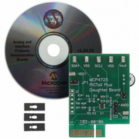
MCP4725DM-PTPLS
Description
BOARD DAUGHTER PICTAIL MCP4725
Manufacturer
Microchip Technology
Specifications of MCP4725DM-PTPLS
Number Of Dac's
1
Number Of Bits
12
Outputs And Type
1, Single Ended
Sampling Rate (per Second)
100k ~ 3.4M
Data Interface
I²C
Settling Time
6µs
Dac Type
Voltage
Voltage Supply Source
Single
Operating Temperature
-40°C ~ 125°C
Utilized Ic / Part
MCP4725
Silicon Manufacturer
Microchip
Application Sub Type
DAC
Kit Application Type
Data Converter
Silicon Core Number
MCP4725
Silicon Family Name
PICtail
Lead Free Status / RoHS Status
Lead free / RoHS Compliant
Available stocks
Company
Part Number
Manufacturer
Quantity
Price
Company:

Part Number:
MCP4725DM-PTPLS
Manufacturer:
Microchip Technology
Quantity:
135


MCP4725
8.2
The user can store the DAC input code (12 bits) and
power-down configuration bits (2 bits) in the internal
non-volatile EEPROM memory using the I
command. The user can also read the EEPROM data
using the I
powered after power is shut down, the device uploads
the
automatically
immediately. This feature is very useful in applications
where the DAC device is used to provide set point or
calibration data for other devices in the application
system. The DAC will not lose the important system
operational parameters due to the system power failure
incidents. See Section 5.6 “Non-Volatile EEPROM
Memory” for more details of the non-volatile EEPROM
memory.
8.3
The power supply to the device is used for both V
and DAC reference voltage. Any noise induced on the
V
application will require a bypass capacitor in order to
filter out high frequency noise on the V
noise can be induced onto the power supply’s traces or
as a result of changes on the DAC output. The bypass
capacitor helps to minimize the effect of these noise
sources on signal integrity.
example of using two bypass capacitors (a 10 µF
tantalum capacitor and a 0.1 µF ceramic capacitor) in
parallel on the V
placed as close to the V
4 mm).
The power source should be as clean as possible. If the
application circuit has separate digital and analog
power supplies, the V
should reside on the analog plane.
DS22039D-page 34
DD
line can affect on the DAC performance. Typical
EEPROM
Using Non-Volatile EEPROM
Memory
Power Supply Considerations
2
C read command. When the device is first
and
DD
contents
line. These capacitors should be
DD
provides
and V
DD
to
SS
pin as possible (within
Figure 8-1
pins of the MCP4725
the
the
DAC
DAC
DD
shows an
line. The
2
C write
register
output
DD
8.4
Inductively-coupled AC transients and digital switching
noise from other devices can affect on DAC
performance and DAC output signal integrity. Careful
board layout will minimize these effects. Bench testing
has shown that a multi-layer board utilizing a low-
inductance ground plane, isolated inputs, isolated
outputs and proper decoupling are critical to achieving
the performance that the MCP4725 is capable of
providing. Particularly harsh environments may require
shielding of critical signals. Separate digital and analog
ground planes are recommended. In this case, the V
pin and the ground pins of the V
MCP4725 should be terminated to the analog ground
plane.
8.5
The MCP4725 is a rail-to-rail output DAC designed to
operate with a V
amplifier is robust enough to drive common, small-
signal loads directly, thus eliminating the cost and size
of an external buffer for most applications.
8.5.1
A common application for the MCP4725 is a digitally-
controlled set point or a calibration of variable
parameters such as sensor offset or bias point.
Example 8-1
Since the MCP4725 is a 12-bit DAC and uses the V
supply as a reference source, it provides a V
resolution per step.
Layout Considerations
Application Examples
DC SET POINT OR CALIBRATION
shows an example of the set point setting.
DD
range of 2.7V to 5.5V. Its output
© 2009 Microchip Technology Inc.
DD
capacitors of the
DD
/4096 of
DD
SS
Related parts for MCP4725DM-PTPLS
Image
Part Number
Description
Manufacturer
Datasheet
Request
R

Part Number:
Description:
Manufacturer:
Microchip Technology Inc.
Datasheet:
Part Number:
Description:
Manufacturer:
Microchip Technology Inc.
Datasheet:
Part Number:
Description:
Manufacturer:
Microchip Technology Inc.
Datasheet:
Part Number:
Description:
Manufacturer:
Microchip Technology Inc.
Datasheet:
Part Number:
Description:
Manufacturer:
Microchip Technology Inc.
Datasheet:
Part Number:
Description:
Manufacturer:
Microchip Technology Inc.
Datasheet:
Part Number:
Description:
Manufacturer:
Microchip Technology Inc.
Datasheet:
Part Number:
Description:
Manufacturer:
Microchip Technology Inc.
Datasheet: