EVAL-AD5415EBZ Analog Devices Inc, EVAL-AD5415EBZ Datasheet - Page 18
EVAL-AD5415EBZ
Manufacturer Part Number
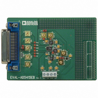
EVAL-AD5415EBZ
Description
BOARD EVALUATION FOR AD5415
Manufacturer
Analog Devices Inc
Specifications of EVAL-AD5415EBZ
Number Of Dac's
2
Number Of Bits
12
Outputs And Type
2, Differential
Sampling Rate (per Second)
2.47M
Data Interface
Serial
Settling Time
120ns
Dac Type
Current
Voltage Supply Source
Single
Operating Temperature
-40°C ~ 125°C
Utilized Ic / Part
AD5415
Lead Free Status / RoHS Status
Lead free / RoHS Compliant


AD5415
REFERENCE SELECTION
When selecting a reference for use with the AD54xx series of
current output DACs, pay attention to the reference’s output
voltage temperature coefficient specification. This parameter
not only affects the full-scale error, but also can affect the
linearity (INL and DNL) performance. The reference tempera-
ture coefficient should be consistent with the system accuracy
specifications. For example, an 8-bit system required to hold its
overall specification to within 1 LSB over the temperature range
0°C to 50°C dictates that the maximum system drift with
temperature should be less than 78 ppm/°C. A 12-bit system
with the same temperature range to overall specification within
2 LSB requires a maximum drift of 10 ppm/°C. Choosing a
precision reference with a low output temperature coefficient
minimizes this error source. Table 7 lists some of the references
available from Analog Devices that are suitable for use with this
range of current output DACs.
AMPLIFIER SELECTION
The primary requirement for the current-steering mode is an
amplifier with low input bias currents and low input offset
voltage. Because of the code-dependent output resistance of the
DAC, the input offset voltage of an op amp is multiplied by the
variable gain of the circuit. A change in this noise gain between
two adjacent digital fractions produces a step change in the
output voltage due to the amplifier’s input offset voltage. This
output voltage change is superimposed on the desired change in
Rev. B | Page 18 of 32
output between the two codes and gives rise to a differential
linearity error, which, if large enough, could cause the DAC to
be nonmonotonic.
The input bias current of an op amp also generates an offset at
the voltage output as a result of the bias current flowing in the
feedback resistor, R
low enough to prevent significant errors in 12-bit applications.
Common-mode rejection of the op amp is important in
voltage-switching circuits, because it produces a code-
dependent error at the voltage output of the circuit. Most op
amps have adequate common-mode rejection for use at 12-bit
resolution.
Provided that the DAC switches are driven from true wideband
low impedance sources (V
Consequently, the slew rate and settling time of a voltage-
switching DAC circuit is largely determined by the output op
amp. To obtain minimum settling time in this configuration,
minimize capacitance at the V
in this application) of the DAC. This is done by using low input
capacitance buffer amplifiers and careful board design.
Most single-supply circuits include ground as part of the analog
signal range, which in turn requires an amplifier that can
handle rail-to-rail signals. Analog Devices offers a wide range of
single-supply amplifiers, as listed in Table 8 and Table 9.
FB
. Most op amps have input bias currents
IN
and AGND), they settle quickly.
REF
node (the voltage output node
Related parts for EVAL-AD5415EBZ
Image
Part Number
Description
Manufacturer
Datasheet
Request
R


Part Number:
Description:
BOARD EVAL FOR SI270X-A
Manufacturer:
Silicon Laboratories Inc
Datasheet:

Part Number:
Description:
BUCK CONV REF DESIGN KIT IP1201
Manufacturer:
International Rectifier
Datasheet:
Part Number:
Description:
BOARD DEMO SYNC DUAL BUCK CNVTER
Manufacturer:
International Rectifier
Datasheet:
Part Number:
Description:
BOARD DEMO SYNC BUCK CONVETER
Manufacturer:
International Rectifier
Datasheet:

Part Number:
Description:
EVALBOARD/EB Omnidirectional microphone - Analog
Manufacturer:
Analog Devices
Datasheet:
Part Number:
Description:
EVALBOARD/EB Omnidirectional microphone - Analog
Manufacturer:
Analog Devices
Datasheet:


Part Number:
Description:
BOARD EVAL LED DRIVER LT3756
Manufacturer:
Linear Technology
Datasheet:

Part Number:
Description:
BOARD EVAL FOR AD7741/7742
Manufacturer:
Analog Devices Inc
Datasheet:

Part Number:
Description:
±1.7g Dual-Axis IMEMS Accelerometer Evaluation Board
Manufacturer:
Analog Devices Inc
Datasheet:

Part Number:
Description:
IC MULTIPLIER ANALOG 8-SOIC T/R
Manufacturer:
Analog Devices Inc
Datasheet:

Part Number:
Description:
IC ANALOG MULTIPLIER 8-DIP
Manufacturer:
Analog Devices Inc
Datasheet:
Part Number:
Description:
IC ANALOG MULTIPLIER 8-SOIC
Manufacturer:
Analog Devices Inc
Datasheet:
Part Number:
Description:
IC ANALOG MULTIPLIER 8-DIP
Manufacturer:
Analog Devices Inc
Datasheet: