DC1319B-A Linear Technology, DC1319B-A Datasheet - Page 12
DC1319B-A
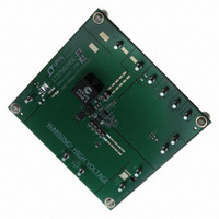
Manufacturer Part Number
DC1319B-A
Description
BOARD EVAL LED DRIVER LT3756
Manufacturer
Linear Technology
Specifications of DC1319B-A
Current - Output / Channel
500mA
Outputs And Type
1, Non-Isolated
Voltage - Output
100V
Features
Dimmable
Voltage - Input
8 ~ 80V
Utilized Ic / Part
LT3756
Lead Free Status / RoHS Status
Lead free / RoHS Compliant
Other names
DC1319A-A
DC1319A-A
DC1319A-A


LT3756/LT3756-1/LT3756-2
When V
lated to:
The LED current programming feature can increase total
dimming range by a factor of 10. The CTRL pin should
not be left open (tie to V
can also be used in conjunction with a thermistor to
provide overtemperature protection for the LED load, or
with a resistor divider to V
switching current when V
varying differential voltage signal (ripple) across ISP and
ISN at the switching frequency is expected. The amplitude
of this signal is increased by high LED load current, low
switching frequency and/or a smaller value output filter
capacitor. Some level of ripple signal is acceptable: the
compensation capacitor on the VC pin filters the signal so
the average difference between ISP and ISN is regulated
to the user-programmed value. Ripple voltage amplitude
(peak-to-peak) in excess of 20mV should not cause mis-
operation, but may lead to noticeable offset between the
average value and the user-programmed value.
Programming Output Voltage (Constant-Voltage
Regulation) or Open LED/Overvoltage Threshold
For a boost or SEPIC application, the output voltage can
be set by selecting the values of R3 and R4 (see Figure 2)
according to the following equation:
For a boost type LED driver, set the resistor from the output
to the FB pin such that the expected V
applicaTions inForMaTion
I
V
LED
OUT
=
CTRL
= 1.25 •
100mV
Figure 2. Feedback Resistor Connection
for Boost or SEPIC LED Drivers
R
LED
is higher than 1.2V, the LED current is regu-
R3 + R4
R4
LT3756
375612 F02
IN
REF
FB
IN
is low. The presence of a time
to reduce output power and
if not used). The CTRL pin
V
IN
R3
R4
FB
during normal
ISP/ISN Short-Circuit Protection Feature (for SEPIC)
The ISP and ISN pins have a protection feature indepen-
dent of the LED current sense feature that operates at
ISN below 3V. The purpose of this feature is to provide
continuous current sensing when ISN is below the LED
current sense common mode range (during start-up or
an output short-circuit fault) to prevent the development
of excessive switching currents that could damage the
power components in a SEPIC converter. The action
threshold (150mV, typ) is above the default LED current
sense threshold, so that no interference will occur over
the ISN voltage range where these two functions overlap.
This feature acts in the same manner as SENSE current
limit — it prevents GATE from going high (switch turn-on)
until the ISP/ISN difference falls below the threshold. If the
load has appreciable series inductance, use of a Schottky
clamp from GND to ISN is recommended for the SEPIC
to prevent excessive current flowing from the ISN pin in
a fault.
Dimming Control
There are two methods to control the current source for
dimming using the LT3756. One method uses the CTRL
pin to adjust the current regulated in the LEDs. A second
operation will not exceed 1.1V. For an LED driver of buck or
a buck-boost configuration, the output voltage is typically
level-shifted to a signal with respect to GND as illustrated
in Figure 3. The output can be expressed as:
V
OUT
LT3756
= V
Figure 3. Feedback Resistor Connection for
Buck Mode or Buck-Boost Mode LED Driver
375612 F03
BE
FB
+ 1.25 •
R3
R4
R3
R4
+
–
V
OUT
100k
R
SEN(EXT)
LED
ARRAY
C
OUT
375612fb
Related parts for DC1319B-A
Image
Part Number
Description
Manufacturer
Datasheet
Request
R

Part Number:
Description:
CD ROM LINEARVIEW DATASHEETS
Manufacturer:
Linear Technology

Part Number:
Description:
Standalone Linear Li-Ion Battery Charger with Thermal Regulation in ThinSOT
Manufacturer:
Linear Technology Corporation
Datasheet:
Part Number:
Description:
Low noise, high frequency, 8th order linear phase lowpass filter
Manufacturer:
Linear Technology Corporation
Datasheet:
Part Number:
Description:
Manufacturer:
Linear Technology Corporation
Datasheet:
Part Number:
Description:
Manufacturer:
Linear Technology Corporation
Datasheet:
Part Number:
Description:
Manufacturer:
Linear Technology Corporation
Datasheet:
Part Number:
Description:
Manufacturer:
Linear Technology Corporation
Datasheet:
Part Number:
Description:
Manufacturer:
Linear Technology Corporation
Datasheet:
Part Number:
Description:
Manufacturer:
Linear Technology Corporation
Datasheet:
Part Number:
Description:
Manufacturer:
Linear Technology Corporation
Datasheet:
Part Number:
Description:
Dual and Quad, JFET Input Precision High Speed Op Amps
Manufacturer:
Linear Technology Corporation
Datasheet:
Part Number:
Description:
Manufacturer:
Linear Technology Corporation
Datasheet:
Part Number:
Description:
1, 2, 6 and 8 Channel, 10-Bit Serial I/O Data Acquisition Systems
Manufacturer:
Linear Technology Corporation
Datasheet:
Part Number:
Description:
Manufacturer:
Linear Technology Corporation
Datasheet:
Part Number:
Description:
Universal dual filter building block
Manufacturer:
Linear Technology Corporation
Datasheet: