LM3501TL-16EV National Semiconductor, LM3501TL-16EV Datasheet - Page 13
LM3501TL-16EV
Manufacturer Part Number
LM3501TL-16EV
Description
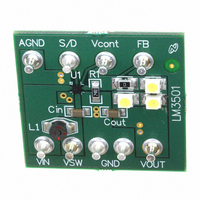
BOARD EVALUATION LM3501TL-16
Manufacturer
National Semiconductor
Series
PowerWise®r
Specifications of LM3501TL-16EV
Current - Output / Channel
20mA
Outputs And Type
1, Non-Isolated
Voltage - Output
16 V
Features
Dimmable
Voltage - Input
2.7 ~ 7V
Utilized Ic / Part
LM3501
Core Chip
LM3501
Topology
Buck
No. Of Outputs
1
Output Voltage
16V
Input Voltage
2.7V To 7V
Development Tool Type
Hardware - Eval/Demo Board
Mcu Supported Families
LM3501
Lead Free Status / RoHS Status
Not applicable / Not applicable


Application Information
ADJUSTING LED CURRENT
The maximum White LED current is set using the following
equation:
The LED current can be controlled using an external DC
voltage. The recommended operating range for the voltage
on the CNTRL pin is 0V to 2.7V. When CNTRL is 2.7V, FB =
0.515V (typ.) The FB voltage will continue to increase if
CNTRL is brought above 2.7V (not recommended). The
CNTRL to FB voltage relationship is:
The LED current can be controlled using a PWM signal on
the SHDN pin with frequencies in the range of 100 Hz
(greater than visible frequency spectrum) to 1 kHz. For
controlling LED currents down to the µA levels, it is best to
use a PWM signal frequency between 200-500 Hz. The
LM3501 LED current can be controlled with PWM signal
frequencies above 1 kHz but the controllable current de-
creases with higher frequency. The maximum LED current
would be achieved using the equation above with 100% duty
cycle, ie. the SHDN pin always high.
Applying a voltage greater than 125 mV to the CNTRL pin
will begin regulating current to the LEDs. A voltage below 75
mV will prevent application or regulation of the LED current.
LED-DRIVE CAPABILITY
The maximum number of LEDs that can be driven by the
LM3501 is limited by the output voltage capability of the
LM3501. When using the LM3501 in the typical application
configuration, with LEDs stacked in series between the V
and FB pins, the maximum number of LEDs that can be
placed in series (N
forward voltage (V
back pin (V
voltage protection level of the chosen LM3501 option
(LM3501-16: OVP
For the circuit to function properly, the following inequality
must be met:
When inserting a value for maximum LED VF, LED forward
voltage variation over the operating temperature range
should be considered. The table below provides maximum
LED voltage numbers for the LM3501-16 and LM3501-21 in
the typical application circuit configuration (with 3, 4, 5, 6, or
7 LEDs placed in series between the V
FB-MAX
(N
MAX
x V
MIN
= 0.545V), and the minimum output over-
F-MAX
MAX
F-MAX
= 15V; LM3501-21: OVP
) is dependent on the maximum LED
), the voltage of the LM3501 feed-
) + 0.545V ≤ OVP
OUT
and FB pins).
MIN
MIN
= 20V).
OUT
13
For the LM3501 to operate properly, the output voltage must
be kept above the input voltage during operation. For most
applications, this requires a minimum of 2 LEDs (total of 6V
or more) between the FB and V
OUTPUT OVERVOLTAGE PROTECTION
The LM3501 contains dedicated circuitry for monitoring the
output voltage. In the event that the primary LED network is
disconnected from the LM3501-16, the output voltage will
increase and be limited to 15.5V (typ.). There is a 900 mV
hysteresis associated with this circuitry which will cause the
output to fluctuate between 15.5V and 14.6V (typ.) if the
primary network is disconnected. In the event that the net-
work is reconnected regulation will begin at the appropriate
output voltage. The 15.5V limit allows the use of 16V 1 µF
ceramic output capacitors creating an overall small solution
for white LED applications.
In the event that the primary LED network is disconnected
from the LM3501-21, the output voltage will increase and be
limited to 20.5V (typ.). There is a 1V hysteresis associated
with this circuitry which will cause the output to fluctuate
between 20.5V and 19.5V (typ.) if the primary network is
disconnected. In the event that the network is reconnected
regulation will begin at the appropriate output voltage. The
20.5V limit allows the use of 25V 1 µF ceramic output
capacitors.
RELIABILITY AND THERMAL SHUTDOWN
The maximum continuous pin current for the 8 pin thin micro
SMD package is 535 mA. When driving the device near its
power output limits the V
than 535 mA (see INDUCTOR SELECTION section for av-
erage switch current). To preserve the long term reliability of
the device the average switch current should not exceed 535
mA.
The LM3501 has an internal thermal shutdown function to
protect the die from excessive temperatures. The thermal
shutdown trip point is typically 150˚C. There is a hysteresis
of typically 35˚C so the die temperature must decrease to
approximately 115˚C before the LM3501 will return to normal
operation.
INDUCTOR SELECTION
The inductor used with the LM3501 must have a saturation
current greater than the cycle by cycle peak inductor current
(see Typical Peak Inductor Currents table below). Choosing
inductors with low DCR decreases power losses and in-
creases efficiency.
# of LEDs
(in series)
3
4
5
6
7
LM3501-16
4.82V
3.61V
2.89V
SW
X
X
pin can see a higher DC current
Maximum LED V
OUT
pins.
LM3501-21
6.49V
4.86V
3.89V
3.24V
2.78V
F
www.national.com
Related parts for LM3501TL-16EV
Image
Part Number
Description
Manufacturer
Datasheet
Request
R

Part Number:
Description:
Synchronous Step-up DC/DC Converter For White Led Applications
Manufacturer:
National Semiconductor Corporation
Datasheet:

Part Number:
Description:
IC LED DRVR WHT BCKLT 8-MICROSMD
Manufacturer:
National Semiconductor
Datasheet:
Part Number:
Description:
IC LED DRVR WHT BCKLT 8-MICROSMD
Manufacturer:
National Semiconductor
Datasheet:
Part Number:
Description:
Synchronous Step-up DC/DC Converter for White LED Applications
Manufacturer:
NSC [National Semiconductor]
Datasheet:

Part Number:
Description:
The LM350 is an adjustable 3-terminal positive voltage regulator capable of supplying in excess of 3
Manufacturer:
Fairchild Semiconductor
Datasheet:

Part Number:
Description:
3.0 A, Adjustable Output, Positive Voltage Regulat
Manufacturer:
On Semiconductor

Part Number:
Description:
National Semiconductor [8-Bit D/A Converter]
Manufacturer:
National Semiconductor
Datasheet:
Part Number:
Description:
National Semiconductor [Media Coprocessor]
Manufacturer:
National Semiconductor
Datasheet:
Part Number:
Description:
Digitally Controlled Tone and Volume Circuit with Stereo Audio Power Amplifier, Microphone Preamp Stage and National 3D Sound
Manufacturer:
National Semiconductor
Datasheet:
Part Number:
Description:
Digitally Controlled Tone and Volume Circuit with Stereo Audio Power Amplifier, Microphone Preamp Stage and National 3D Sound
Manufacturer:
National Semiconductor
Datasheet:
Part Number:
Description:
AC97 Rev 2 Codec with Sample Rate Conversion and National 3D Sound
Manufacturer:
National Semiconductor
Part Number:
Description:
Manufacturer:
National Semiconductor
Datasheet:
Part Number:
Description:
Manufacturer:
National Semiconductor
Datasheet: