LM3501TL-16EV National Semiconductor, LM3501TL-16EV Datasheet - Page 14
LM3501TL-16EV
Manufacturer Part Number
LM3501TL-16EV
Description
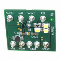
BOARD EVALUATION LM3501TL-16
Manufacturer
National Semiconductor
Series
PowerWise®r
Specifications of LM3501TL-16EV
Current - Output / Channel
20mA
Outputs And Type
1, Non-Isolated
Voltage - Output
16 V
Features
Dimmable
Voltage - Input
2.7 ~ 7V
Utilized Ic / Part
LM3501
Core Chip
LM3501
Topology
Buck
No. Of Outputs
1
Output Voltage
16V
Input Voltage
2.7V To 7V
Development Tool Type
Hardware - Eval/Demo Board
Mcu Supported Families
LM3501
Lead Free Status / RoHS Status
Not applicable / Not applicable


www.national.com
Application Information
The minimum inductor value required for the LM3501-16 can
be calculated using the following equation:
The minimum inductor value required for the LM3501-21 can
be calculated using the following equation:
For both equations above, L is in µH, V
of the chip in Volts, R
power switch found in the Typical Performance Characteris-
tics section in ohms and D is the duty cycle of the switching
regulator. The above equation is only valid for D greater than
or equal to 0.5. For applications where the minimum duty
cycle is less than 0.5, a 22 µH inductor is the typical recom-
mendation for use with most applications. Bench-level veri-
fication of circuit performance is required in these special
cases, however. The duty cycle, D, is given by the following
equation:
where V
Note 10: C
L = 22 µH, 160 mΩ DCR max. Coilcraft DT1608C-223
2 and 3 LED applications: LM3501-16 or LM3501-21; LED V
20mA; T
4 LED applications: LM3501-16 or LM3501-21; LED V
= 25˚C
5 LED applications: LM3501-21 only; LED V
VIN
(V)
2.7
3.3
4.2
Typical Peak Inductor Current (mA)(Note 10)
A
= 25˚C
OUT
IN
# LEDs
series)
= C
(in
is the voltage at pin C1.
2
3
4
5
2
3
4
5
2
3
4
5
OUT
= 1 µF
DSON
142
191
132
183
102
122
179
mA
118
110
15
82
76
64
is the ON resistance of the NMOS
mA
100
138
174
232
126
158
216
146
206
116
20
90
76
LED Current
mA
134
190
244
319
116
168
212
288
148
186
263
30
96
F
= 3.28V at 20mA; T
IN
mA
160
244
322
413
136
210
270
365
116
180
232
324
40
is the input supply
(Continued)
F
= 3.41V at 20mA; T
204
294
172
250
320
446
142
210
272
388
mA
50
X
X
F
= 3.77V at
A
mA
234
352
198
290
162
246
318
456
= 25˚C
60
X
X
X
X
A
14
The typical cycle-by-cycle peak inductor current can be cal-
culated from the following equation:
where I
frequency, L is the inductance and η is the converter effi-
ciency of the total driven load. A good typical number to use
for η is 0.8. The value of η can vary with load and duty cycle.
The average inductor current, which is also the average V
pin current, is given by the following equation:
The maximum output current capability of the LM3501 can
be estimated with the following equation:
where I
include but are not limited to:
Coilcraft DT1608C series
Coilcraft DO1608C series
TDK VLP4612 series
TDK VLP5610 series
TDK VLF4012A series
CAPACITOR SELECTION
Choose low ESR ceramic capacitors for the output to mini-
mize output voltage ripple. Multilayer X7R or X5R type ce-
ramic capacitors are the best choice. For most applications,
a 1 µF ceramic output capacitor is sufficient.
Local bypassing for the input is needed on the LM3501.
Multilayer X7R or X5R ceramic capacitors with low ESR are
a good choice for this as well. A 1 µF ceramic capacitor is
sufficient for most applications. However, for some applica-
tions at least a 4.7 µF ceramic capacitor may be required for
proper startup of the LM3501. Using capacitors with low
ESR decreases input voltage ripple. For additional bypass-
ing, a 100 nF ceramic capacitor can be used to shunt high
frequency ripple on the input. Some recommended capaci-
tors include but are not limited to:
TDK C2012X7R1C105K
Taiyo-Yuden EMK212BJ105 G
LAYOUT CONSIDERATIONS
The input bypass capacitor C
be placed close to the device and connect between the V
and GND pins. This will reduce copper trace resistance
which effects the input voltage ripple of the IC. For additional
input voltage filtering, a 100 nF bypass capacitor can be
placed in parallel with C
to ground. The output capacitor, C
close to the LM3501 and connected directly between the
V
C
directly effects output voltage ripple and efficiency. The cur-
rent setting resistor, R
OUT
OUT
and GND pins. Any copper trace connections for the
capacitor can increase the series resistance, which
CL
OUT
is the current limit. Some recommended inductors
is the total load current, F
LED
IN
, should be kept close to the FB pin
to shunt any high frequency noise
IN
, as shown in Figure 2, must
OUT
, should also be placed
SW
is the switching
SW
IN
Related parts for LM3501TL-16EV
Image
Part Number
Description
Manufacturer
Datasheet
Request
R

Part Number:
Description:
Synchronous Step-up DC/DC Converter For White Led Applications
Manufacturer:
National Semiconductor Corporation
Datasheet:

Part Number:
Description:
IC LED DRVR WHT BCKLT 8-MICROSMD
Manufacturer:
National Semiconductor
Datasheet:
Part Number:
Description:
IC LED DRVR WHT BCKLT 8-MICROSMD
Manufacturer:
National Semiconductor
Datasheet:
Part Number:
Description:
Synchronous Step-up DC/DC Converter for White LED Applications
Manufacturer:
NSC [National Semiconductor]
Datasheet:

Part Number:
Description:
The LM350 is an adjustable 3-terminal positive voltage regulator capable of supplying in excess of 3
Manufacturer:
Fairchild Semiconductor
Datasheet:

Part Number:
Description:
3.0 A, Adjustable Output, Positive Voltage Regulat
Manufacturer:
On Semiconductor

Part Number:
Description:
National Semiconductor [8-Bit D/A Converter]
Manufacturer:
National Semiconductor
Datasheet:
Part Number:
Description:
National Semiconductor [Media Coprocessor]
Manufacturer:
National Semiconductor
Datasheet:
Part Number:
Description:
Digitally Controlled Tone and Volume Circuit with Stereo Audio Power Amplifier, Microphone Preamp Stage and National 3D Sound
Manufacturer:
National Semiconductor
Datasheet:
Part Number:
Description:
Digitally Controlled Tone and Volume Circuit with Stereo Audio Power Amplifier, Microphone Preamp Stage and National 3D Sound
Manufacturer:
National Semiconductor
Datasheet:
Part Number:
Description:
AC97 Rev 2 Codec with Sample Rate Conversion and National 3D Sound
Manufacturer:
National Semiconductor
Part Number:
Description:
Manufacturer:
National Semiconductor
Datasheet:
Part Number:
Description:
Manufacturer:
National Semiconductor
Datasheet: