LM3423MHBKBSTEV/NOPB National Semiconductor, LM3423MHBKBSTEV/NOPB Datasheet - Page 14
LM3423MHBKBSTEV/NOPB
Manufacturer Part Number
LM3423MHBKBSTEV/NOPB
Description
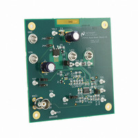
BOARD EVAL BUCK BOOST LM3423
Manufacturer
National Semiconductor
Series
PowerWise®r
Specifications of LM3423MHBKBSTEV/NOPB
Current - Output / Channel
1A
Outputs And Type
1, Non-Isolated
Voltage - Output
35V
Features
Dimmable
Voltage - Input
4.5 ~ 35V
Utilized Ic / Part
LM3423
Lead Free Status / RoHS Status
Lead free / RoHS Compliant
Other names
LM3423MHBKBSTEV


www.national.com
CONTROL LOOP COMPENSATION
The LM3421/23 control loop is modeled like any current mode
controller. Using a first order approximation, the uncompen-
sated loop can be modeled as a single pole created by the
output capacitor and, in the boost and buck-boost topologies,
a right half plane zero created by the inductor, where both
have a dependence on the LED string dynamic resistance.
There is also a high frequency pole in the model, however it
is near the switching frequency and plays no part in the com-
pensation design process therefore it will be neglected. Since
ceramic capacitance is recommended for use with LED
drivers due to long lifetimes and high ripple current rating, the
ESR of the output capacitor can also be neglected in the loop
analysis. Finally, there is a DC gain of the uncompensated
loop which is dependent on internal controller gains and the
external sensing network.
A buck-boost regulator will be used as an example case. See
the Design Guide section for compensation of all topologies.
The uncompensated loop gain for a buck-boost regulator is
given by the following equation:
Where the uncompensated DC loop gain of the system is de-
scribed as:
And the output pole (ω
P1
) is approximated:
FIGURE 9. Compensation Circuitry
14
And the right half plane zero (ω
Figure 8
scenario when the RHP zero is below the output pole. This
occurs at high duty cycles when the regulator is trying to boost
the output voltage significantly. The RHP zero adds 20dB/
decade of gain while loosing 45°/decade of phase which
places the crossover frequency (when the gain is zero dB)
extremely high because the gain only starts falling again due
to the high frequency pole (not modeled or shown in figure).
The phase will be below -180° at the crossover frequency
which means there is no phase margin (180° + phase at
crossover frequency) causing system instability. Even if the
output pole is below the RHP zero, the phase will still reach
-180° before the crossover frequency in most cases yielding
instability.
FIGURE 8. Uncompensated Loop Gain Frequency
shows the uncompensated loop gain in a worst-case
Response
Z1
) is:
300673a3
300673a7
Related parts for LM3423MHBKBSTEV/NOPB
Image
Part Number
Description
Manufacturer
Datasheet
Request
R

Part Number:
Description:
National Semiconductor [8-Bit D/A Converter]
Manufacturer:
National Semiconductor
Datasheet:
Part Number:
Description:
National Semiconductor [Media Coprocessor]
Manufacturer:
National Semiconductor
Datasheet:
Part Number:
Description:
Digitally Controlled Tone and Volume Circuit with Stereo Audio Power Amplifier, Microphone Preamp Stage and National 3D Sound
Manufacturer:
National Semiconductor
Datasheet:
Part Number:
Description:
Digitally Controlled Tone and Volume Circuit with Stereo Audio Power Amplifier, Microphone Preamp Stage and National 3D Sound
Manufacturer:
National Semiconductor
Datasheet:
Part Number:
Description:
AC97 Rev 2 Codec with Sample Rate Conversion and National 3D Sound
Manufacturer:
National Semiconductor
Part Number:
Description:
Manufacturer:
National Semiconductor
Datasheet:
Part Number:
Description:
Manufacturer:
National Semiconductor
Datasheet:
Part Number:
Description:
General Purpose, Low Voltage, Low Power, Rail-to-Rail Output Operational Amplifiers
Manufacturer:
National Semiconductor
Datasheet:
Part Number:
Description:
8-bit 20 MSPS flash A/D converter.
Manufacturer:
National Semiconductor
Datasheet:
Part Number:
Description:
Low Noise Quad Operational Amplifier
Manufacturer:
National Semiconductor
Datasheet:
Part Number:
Description:
Quad Differential Line Receivers
Manufacturer:
National Semiconductor
Datasheet:
Part Number:
Description:
Quad High Speed Trapezoidal? Bus Transceiver
Manufacturer:
National Semiconductor
Datasheet:
Part Number:
Description:
Dual Line Receiver
Manufacturer:
National Semiconductor
Datasheet:
Part Number:
Description:
TTL to 10k ECL Level Translator with Latch
Manufacturer:
National Semiconductor
Datasheet: