NCP5006EVB ON Semiconductor, NCP5006EVB Datasheet - Page 3
NCP5006EVB
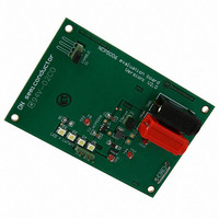
Manufacturer Part Number
NCP5006EVB
Description
EVAL BOARD FOR NCP5006
Manufacturer
ON Semiconductor
Specifications of NCP5006EVB
Design Resources
NCP5006 Demo Board BOM NCP5006EVB Gerber Files NCP5006 Demo Board Schematic
Current - Output / Channel
15mA
Outputs And Type
1, Non-Isolated
Voltage - Output
22V
Voltage - Input
3.6V
Utilized Ic / Part
NCP5006
Core Chip
NCP5006
Topology
Boost
No. Of Outputs
1
Development Tool Type
Hardware - Eval/Demo Board
Mcu Supported Families
NCP5006
Lead Free Status / RoHS Status
Lead free / RoHS Compliant
Features
-
Lead Free Status / Rohs Status
Lead free / RoHS Compliant
For Use With/related Products
NCP5006
Other names
NCP5006EVBOS


PIN FUNCTION DESCRIPTION
Pin
1
2
3
4
5
Pin Name
GND
V
V
FB
EN
out
bat
ANALOG INPUT
DIGITAL INPUT
POWER
POWER
POWER
Type
This pin is the power side of the external inductor and must be connected to the
external Schottky diode. It provides the output current to the load. Since the boost
converter operates in a current loop mode, the output voltage can range up to
+24 V but shall not extend this limit. However, if the voltage on this pin is higher
than the Over Voltage Protection threshold (OVP) the device comes back to
shutdown mode. To restart the chip, one must either send a Low to High
sequence on Pin EN, or switch off the V
the output voltage to avoid false triggering of the OVP circuit. This capacitor
should be 1.0 mF minimum. Ceramic type, (ESR <100 mW), is mandatory to
achieve the high end efficiency. This capacitor limits the noise created by the fast
transients present in this circuitry. In order to limit the inrush current and to
operate with an acceptable start−up time, it is recommended to use any value
between 1.0 mF and 8.2 mF capacitor maximum. Care must be observed to avoid
EMI through the PCB copper tracks connected to this pin.
This pin is the system ground for the NCP5006 and carries both the power and
the analog signals. High quality ground must be provided to avoid spikes and/or
uncontrolled operation. Care must be observed to avoid high−density current flow
in a limited PCB copper track. Ground plane technique is recommended.
This pin provides the output current range adjustment by means of a sense
resistor connected to the analog control or with a PWM control. The dimming
function can be achieved by applying a PWM voltage technique to this pin (see
Figure 29). The current output tolerance depends upon the accuracy of this
resistor. Using a "5% metal film resistor or better, yields a good enough output
current accuracy.
Note: A built−in comparator switch OFF the DC/DC converter if the voltage
sensed across this pin and ground is higher than 700 mV (typical).
This is an Active−High logic input which enables the boost converter. The built−in
pull down resistor disables the device when the EN pin is left open. The LED
brightness can be controlled by applying a pulse width modulated signal to the
enable pin (see Figure 31).
The external voltage supply is connected to this pin. A high quality reservoir
capacitor must be connected across Pin 1 and Ground to achieve the specified
output voltage parameters. A 4.7 mF/6.3 V, low ESR capacitor must be connected
as close as possible across Pin 5 and ground Pin 2. The X5R or X7R ceramic
MURATA types are recommended. The return side of the external inductor shall
be connected to this pin. Typical application will use a 22 mH, size 1008, to handle
the 1.0 to 100 mA max output current range. On the other hand, when the desired
output current is above 20 mA, the inductor shall have an ESR < 1.5 W to achieve
a good efficiency over the V
http://onsemi.com
NCP5006
3
bat
range.
Description
bat
supply. A capacitor must be used on
Related parts for NCP5006EVB
Image
Part Number
Description
Manufacturer
Datasheet
Request
R

Part Number:
Description:
Compact Backlight LED Boost Driver
Manufacturer:
ON Semiconductor
Datasheet:
Part Number:
Description:
ON Semiconductor [VOLTAGE REGULATOR]
Manufacturer:
ON Semiconductor
Datasheet:
Part Number:
Description:
357-036-542-201 CARDEDGE 36POS DL .156 BLK LOPRO
Manufacturer:
ON Semiconductor
Datasheet:
Part Number:
Description:
357-036-542-201 CARDEDGE 36POS DL .156 BLK LOPRO
Manufacturer:
ON Semiconductor
Datasheet:
Part Number:
Description:
357-036-542-201 CARDEDGE 36POS DL .156 BLK LOPRO
Manufacturer:
ON Semiconductor
Datasheet:
Part Number:
Description:
357-036-542-201 CARDEDGE 36POS DL .156 BLK LOPRO
Manufacturer:
ON Semiconductor
Datasheet:
Part Number:
Description:
357-036-542-201 CARDEDGE 36POS DL .156 BLK LOPRO
Manufacturer:
ON Semiconductor
Datasheet:
Part Number:
Description:
357-036-542-201 CARDEDGE 36POS DL .156 BLK LOPRO
Manufacturer:
ON Semiconductor
Datasheet:
Part Number:
Description:
357-036-542-201 CARDEDGE 36POS DL .156 BLK LOPRO
Manufacturer:
ON Semiconductor
Datasheet:
Part Number:
Description:
357-036-542-201 CARDEDGE 36POS DL .156 BLK LOPRO
Manufacturer:
ON Semiconductor
Datasheet:
Part Number:
Description:
357-036-542-201 CARDEDGE 36POS DL .156 BLK LOPRO
Manufacturer:
ON Semiconductor
Datasheet:
Part Number:
Description:
357-036-542-201 CARDEDGE 36POS DL .156 BLK LOPRO
Manufacturer:
ON Semiconductor
Datasheet:
Part Number:
Description:
Manufacturer:
ON Semiconductor
Datasheet:
Part Number:
Description:
Manufacturer:
ON Semiconductor
Datasheet: