NCP1028LEDGEVB ON Semiconductor, NCP1028LEDGEVB Datasheet - Page 12
NCP1028LEDGEVB
Manufacturer Part Number
NCP1028LEDGEVB
Description
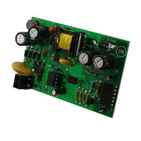
EVAL BOARD FOR NCP1028LEDG
Manufacturer
ON Semiconductor
Specifications of NCP1028LEDGEVB
Design Resources
NCP1028LEDGEVB BOM CP1028LEDGEVB Gerber Files NCP1028LED EVB Schematic
Current - Output / Channel
720mA
Outputs And Type
1, Isolated
Voltage - Output
18V
Voltage - Input
90 ~ 265VAC
Utilized Ic / Part
NCP1028
Core Chip
NCP1028
Topology
Flyback
No. Of Outputs
1
Output Current
720mA
Output Voltage
18V
Development Tool Type
Hardware - Eval/Demo Board
Leaded Process Compatible
Yes
Mcu Supported Families
NCP1028
Rohs Compliant
Yes
Lead Free Status / RoHS Status
Lead free / RoHS Compliant
Features
-
Lead Free Status / Rohs Status
Lead free / RoHS Compliant
For Use With/related Products
NCP1028LEDG
Other names
NCP1028LEDGEVBOS


the output voltage to its target value. We know that the
switcher consumption is around 2.0 mA (I
we can calculate the amount of capacitance we need, to
hold V
2.0 mA:
capacitor.
Fault Condition – Short-Circuit on V
occur between V
(V
device will seriously increase the junction temperature. For
instance, since IC1 equals 3.0 mA (the min corresponds to
the highest T
1.1 W. To avoid this situation, the controller includes a
novel circuitry made of two startup levels, IC1 and IC2. At
powerup, as long as V
delivers IC1 (around 650 mA typical), then, when V
reaches 1.3 V, the source smoothly transitions to IC2 and
delivers its nominal value. As a result, in case of
short-circuit between V
will drop to 370
this particular behavior.
C w 2m · 10 m
Suppose our power supply takes 10 ms (t
In some fault situations, a short-circuit can purposely
C w
HV
= 370 V
CC
I CC1 t startup
1
above 7.5 V at least for 10 ms while delivering
DV CC
J
), the device would dissipate 370
DC
w 20 mF
CC
) the current delivered by the startup
or, by replacing with the above values,
650 m = 240 mW. Figure 25 portrays
and GND. In high line conditions
CC
CC
then select a 33 mF for the V
is below a 1.3 V level, the source
and GND, the power dissipation
Figure 24. A typical startup sequence showing the V
CC1
startup
CC
). Therefore,
) to bring
voltage evolution versus time.
http://onsemi.com
3 m =
CC
CC
NCP1028
12
C
startup time for the first sequence (t
sequence (t
with a delta V of VCC
which finally leads to a second startup time of
7
66 m + 39 m = 105 ms as a typical value. Please note that
this calculation is approximated by the presence of the knee
in the vicinity of the transition.
The first startup period is calculated by the formula
33 m/6.0 m = 39 ms. The total startup time becomes
Figure 25. The startup source now features a
V = I
2
) is obtained by toggling the source to 4.0 mA
t, which implies a 33 m
dual-level startup current.
CC
ON
capacitor
– VCCth = 8.5 – 1.5 = 7.0 V,
1.3/650 m = 66 ms
1
). The second
Related parts for NCP1028LEDGEVB
Image
Part Number
Description
Manufacturer
Datasheet
Request
R

Part Number:
Description:
Low Dropout Linear Regulator Controller
Manufacturer:
ON Semiconductor
Datasheet:

Part Number:
Description:
EVAL BOARD FOR NCP102MBG
Manufacturer:
ON Semiconductor
Datasheet:
Part Number:
Description:
ON Semiconductor [VOLTAGE REGULATOR]
Manufacturer:
ON Semiconductor
Datasheet:
Part Number:
Description:
357-036-542-201 CARDEDGE 36POS DL .156 BLK LOPRO
Manufacturer:
ON Semiconductor
Datasheet:
Part Number:
Description:
357-036-542-201 CARDEDGE 36POS DL .156 BLK LOPRO
Manufacturer:
ON Semiconductor
Datasheet:
Part Number:
Description:
357-036-542-201 CARDEDGE 36POS DL .156 BLK LOPRO
Manufacturer:
ON Semiconductor
Datasheet:
Part Number:
Description:
357-036-542-201 CARDEDGE 36POS DL .156 BLK LOPRO
Manufacturer:
ON Semiconductor
Datasheet:
Part Number:
Description:
357-036-542-201 CARDEDGE 36POS DL .156 BLK LOPRO
Manufacturer:
ON Semiconductor
Datasheet:
Part Number:
Description:
357-036-542-201 CARDEDGE 36POS DL .156 BLK LOPRO
Manufacturer:
ON Semiconductor
Datasheet:
Part Number:
Description:
357-036-542-201 CARDEDGE 36POS DL .156 BLK LOPRO
Manufacturer:
ON Semiconductor
Datasheet:
Part Number:
Description:
357-036-542-201 CARDEDGE 36POS DL .156 BLK LOPRO
Manufacturer:
ON Semiconductor
Datasheet:
Part Number:
Description:
357-036-542-201 CARDEDGE 36POS DL .156 BLK LOPRO
Manufacturer:
ON Semiconductor
Datasheet:
Part Number:
Description:
357-036-542-201 CARDEDGE 36POS DL .156 BLK LOPRO
Manufacturer:
ON Semiconductor
Datasheet:
Part Number:
Description:
Manufacturer:
ON Semiconductor
Datasheet: