MCP1650DM-LED2 Microchip Technology, MCP1650DM-LED2 Datasheet - Page 15
MCP1650DM-LED2
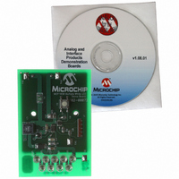
Manufacturer Part Number
MCP1650DM-LED2
Description
BOARD DEMO FOR MCP1650 WHITE LED
Manufacturer
Microchip Technology
Datasheets
1.MCP1650S-EMS.pdf
(28 pages)
2.MCP1650DM-LED2.pdf
(24 pages)
3.MCP9700T-ELT.pdf
(36 pages)
Specifications of MCP1650DM-LED2
Current - Output / Channel
15mA
Outputs And Type
1, Non-Isolated
Voltage - Output
32.4V
Features
Dimmable
Voltage - Input
2.7 ~ 4.5V
Utilized Ic / Part
MCP1650
Core Chip
MCP1650
Topology
Boost
Output Current
560mA
No. Of Outputs
1
Input Voltage
2.7V To 5.5V
Kit Contents
Board
Development Tool Type
Hardware - Eval/Demo Board
Rohs Compliant
Yes
Lead Free Status / RoHS Status
Contains lead / RoHS non-compliant


© 2005 Microchip Technology Inc.
When selecting the MOSFET, a low R
Since the input voltage ranges from 2.7V to 4.5V, the MOSFET must have a turn-on
voltage as low as 2.7V. Ideally, the MOSFET would have R
therefore, help increase the overall efficiency of the regulator. However, a lower R
typically results in higher gate charge, leading to slower transition times in the
MOSFET, thereby causing increased switching losses. The MOSFET’s drain-to-source
breakdown voltage must be rated to handle the boost output voltage plus margin. There
is a very limited selection for MOSFET's with a drain to source rating greater than 30V
with a gate-to-source voltage less than 5V. By using a 1:1 coupled inductor for the boost
converter, the MOSFET drain-to-source voltage rating is cut in half.
The boost diode requires very fast turn-on and turn-off characteristics because it
switches at the switching frequency of the converter. Schottky diodes are recom-
mended because they are capable of this switching characteristic and have a low
forward drop. As with the MOSFET, the Schottky diode must be rated to handle the
boost output voltage plus margin.
The input and output capacitor size depends on the respective voltages of the
converter. While low value parts are desired because of cost and size, they typically
result in higher ripple voltages. The capacitors should be chosen to provide an
appropriate ripple voltage for the intended application. Ceramic or low effective series
resistance (ESR) tantalum capacitors are appropriate for most applications.
2.3.5
The PIC10F202 comes with preprogrammed firmware to operate the system as
described above. The firmware flow diagram is shown in Appendix C. “Demo Board
Firmware”.
There is an initialization routine at the beginning of the program. The program initially
checks for the key press and goes into Sleep mode if there is no key press. The device
will come out of Sleep mode on pin change. The OPTION register is configured to
wake-up on port pin change.
The GPIO port is configured to set GP0 (PWM to the MCP1650) as an output and GP3
(Push Button) as inputs. There are three different subroutines for the three different
intensities provided. Every time the key is pressed, the variable key buffer is incre-
mented to store the next value of the key and move to the respective subroutine in a
cyclic order.
The effect of key de-bounce is accomplished by providing a delay which checks for the
prerequisite time and recognizes only a valid key press. There is a key press check in
each of the subroutine which recognizes the key press and goes to the next subroutine
for a valid key press.
2.3.5.1
Header J1 is provided for in circuit programming. This is an optional feature since the
demo board comes preprogrammed with firmware to operate the system. The
PIC10F202 can be reprogrammed with the Baseline Flash Microcontroller Programmer
(BFMP).
Firmware
PROGRAMMING
Installation and Operation
DSon
logic-level N-channel is recommended.
DSon
as low as possible and,
DS51586A-page 11
DSon
Related parts for MCP1650DM-LED2
Image
Part Number
Description
Manufacturer
Datasheet
Request
R

Part Number:
Description:
BOARD DEMO FOR MCP1650 SEPIC
Manufacturer:
Microchip Technology
Datasheet:

Part Number:
Description:
BOARD DEMO FOR MCP165X
Manufacturer:
Microchip Technology
Datasheet:

Part Number:
Description:
Manufacturer:
Microchip Technology Inc.
Datasheet:
Part Number:
Description:
Manufacturer:
Microchip Technology Inc.
Datasheet:
Part Number:
Description:
Manufacturer:
Microchip Technology Inc.
Datasheet:
Part Number:
Description:
Manufacturer:
Microchip Technology Inc.
Datasheet:
Part Number:
Description:
Manufacturer:
Microchip Technology Inc.
Datasheet:
Part Number:
Description:
Manufacturer:
Microchip Technology Inc.
Datasheet:
Part Number:
Description:
Manufacturer:
Microchip Technology Inc.
Datasheet:
Part Number:
Description:
Manufacturer:
Microchip Technology Inc.
Datasheet: