LX1991 EVAL KIT Microsemi Analog Mixed Signal Group, LX1991 EVAL KIT Datasheet - Page 2
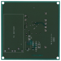
LX1991 EVAL KIT
Manufacturer Part Number
LX1991 EVAL KIT
Description
KIT EVALUATION FOR LED DRIVER
Manufacturer
Microsemi Analog Mixed Signal Group
Specifications of LX1991 EVAL KIT
Current - Output / Channel
30mA
Outputs And Type
6, Non-Isolated
Voltage - Output
40V
Features
Dimmable
Voltage - Input
4.5 ~ 5.5V
Utilized Ic / Part
LX1991
Lead Free Status / RoHS Status
Lead free / RoHS Compliant
Other names
57706
LX1991-EVAL
LX1991EVALKIT
LX1991EVALKIT
LXE1991-01 EVAL KIT
LXE1991-01EVALKIT
LXE1991-01EVALKIT
LX1991-EVAL
LX1991EVALKIT
LX1991EVALKIT
LXE1991-01 EVAL KIT
LXE1991-01EVALKIT
LXE1991-01EVALKIT


Copyright © 2001
Rev. 1.1, 10/27/2005
P
Supply Voltage (VDD ) ............................................................................... -0.3v to 6V
Analog Output Voltage (SINK
Analog Inputs (I
Digital Inputs (ENABLE, DIG_DIM) ...........................................-0.3V to VDD +0.5V
Operating Temperature Range ...................................................................-40°C – 85°C
Storage Temperature Range.....................................................................-65°C – 150°C
Maximum Junction Temperature .......................................................................... 150°C
Peak Package Solder Reflow Temp. (40 seconds max. exposure) ........... 260°C (+0, -5)
Note:
Ground. Currents are positive into, negative out of specified terminal.
DIG_DIM
IN
ENABLE
Junction Temperature Calculation: T
The θ
board system. All of the above assume no ambient airflow.
The θ
SINK
C
T
T
SINK
LQ
GND
I
I
V
N
SLOPE
SET+
HERMAL RESISTANCE
HERMAL RESISTANCE
SET-
DD
AME
JA
JA
1
TM
Exceeding these ratings could cause damage to the device. All voltages are with respect to
6
–
numbers are guidelines for the thermal performance of the device/ 4 layer pc-
numbers are to MIL-STD-883D Method 1012.1
Plastic 4x4 MLPQ 16-Pin
Ground
Voltage Input, 4.5 to 5.5V input range. V
Current sink channels one through six. Each output sinks the programmed current from the V
ground. Compliance voltage is from 1 volt minimum to the V
A logic input that duty cycle modulates the output currents. All output currents are turned on at the programmed
current value when DIG_DIM is high and turned off when it is low. Compatible with both 3V and 5V logic.
Chip Enable Input. If logic high, all functions are enabled. If logic low, internal power is disconnected from the
V
Maximum current into VDD when ENABLE < 0.4V is 1 µA .
Current programming resistor pins. Output current in each channel is 24 times the current that flows from I
I
Current rise and fall time programming capacitor. Rise and fall times increase in direct proportion to capacitor
value. C = 450
SET-
SET
DD
A B S O L U T E M A X I M U M R A T I N G S
).......................................................................-0.3V to VDD +0.5V
pin, disabling all functions. Logic threshold is 1.6 ± 0.8V maximum over supply and temperature range.
I
SET
11861 Western Avenue, Garden Grove, CA. 92841, 714-898-8121, Fax: 714-893-2570
current is 1.26V / R
-
-
JUNCTION TO
JUNCTION TO
1
µ
to SINK
T H E R M A L D A T A
A * T
J
= T
R
6
or T
F U N C T I O N A L P I N D E S C R I P T I O N
A
)............................................... -0.3V to 43V
+ (P
A
A
F
MBIENT
MBIENT
SET
in microseconds, C in picofarads.
D
x θ
. Connect resistor between I
JA
, θ
, θ
).
Integrated Products
®
J
JA
Microsemi
C
DD
is internally switched (see ENABLE) to remove power from chip.
Six Output Programmable LED Current Sink
D
ESCRIPTION
2.2°C/W
36°C/W
LED
SET+
P
supply maximum.
RODUCTION
and I
SET-
RoHS / Pb-free 100% Matte Tin Lead Finish
D
DIG _DIM
ATA
P A C K A G E P I N O U T
SINK 1
SINK 2
xxxx Denotes Date Code / Lot Code
VDD
S
LQ P
HEET
1
3
4
2
16
LQ P
ACKAGE
5
(Top View)
MSC
1991
xxxx
15
6
LED
ACKAGE
14
7
M
supply to
ARKING
13
8
12
11
10
9
LX1991
NC
ISET -
SINK 6
GND
SET+
Page 2
to
Related parts for LX1991 EVAL KIT
Image
Part Number
Description
Manufacturer
Datasheet
Request
R

Part Number:
Description:
BOARD EVAL LED DRIVER 6 CHANNEL
Manufacturer:
Microsemi Analog Mixed Signal Group
Datasheet:

Part Number:
Description:
BOARD EVAL LED DRIVER 6CHANNEL
Manufacturer:
Microsemi Analog Mixed Signal Group
Datasheet:

Part Number:
Description:
Six Output Programmable Led Current Sink
Manufacturer:
Microsemi Corporation
Datasheet:

Part Number:
Description:
IC USB LINE TERM EMI/ESD SC70-6
Manufacturer:
Microsemi Analog Mixed Signal Group
Datasheet:
Part Number:
Description:
IC USB LINE TERM EMI/ESD SC70-6
Manufacturer:
Microsemi Analog Mixed Signal Group
Datasheet:

Part Number:
Description:
IC TERM SCSI 9LINE MODE 24TSSOP
Manufacturer:
Microsemi Analog Mixed Signal Group
Datasheet:

Part Number:
Description:
IC TERM SCSI 9LINE MODE 28TSSOP
Manufacturer:
Microsemi Analog Mixed Signal Group
Datasheet:

Part Number:
Description:
IC TERM SCSI 9LINE LVD 24TSSOP
Manufacturer:
Microsemi Analog Mixed Signal Group
Datasheet:
Part Number:
Description:
IC TERM SCSI 9LINE MODE 36QSOP
Manufacturer:
Microsemi Analog Mixed Signal Group
Datasheet:

Part Number:
Description:
IC USB LINE TERM EMI/ESD SOT23-6
Manufacturer:
Microsemi Analog Mixed Signal Group
Datasheet:

Part Number:
Description:
IC USB LINE TERM EMI/ESD SOT23-6
Manufacturer:
Microsemi Analog Mixed Signal Group
Datasheet:

Part Number:
Description:
IC USB EMI FLTR ESD PROT SOT23-6
Manufacturer:
Microsemi Analog Mixed Signal Group
Part Number:
Description:
IC USB LINE TERM EMI/ESD SOT23-6
Manufacturer:
Microsemi Analog Mixed Signal Group
Datasheet:
Part Number:
Description:
IC AMP AUDIO PWR 10W STER 44SSOP
Manufacturer:
Microsemi Analog Mixed Signal Group
Datasheet:

Part Number:
Description:
IC CHARGER BATT USB LI-ION 20MLP
Manufacturer:
Microsemi Analog Mixed Signal Group
Datasheet: