LX1991 EVAL KIT Microsemi Analog Mixed Signal Group, LX1991 EVAL KIT Datasheet - Page 6
LX1991 EVAL KIT
Manufacturer Part Number
LX1991 EVAL KIT
Description
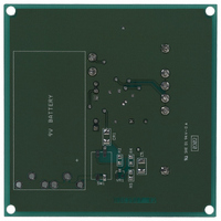
KIT EVALUATION FOR LED DRIVER
Manufacturer
Microsemi Analog Mixed Signal Group
Specifications of LX1991 EVAL KIT
Current - Output / Channel
30mA
Outputs And Type
6, Non-Isolated
Voltage - Output
40V
Features
Dimmable
Voltage - Input
4.5 ~ 5.5V
Utilized Ic / Part
LX1991
Lead Free Status / RoHS Status
Lead free / RoHS Compliant
Other names
57706
LX1991-EVAL
LX1991EVALKIT
LX1991EVALKIT
LXE1991-01 EVAL KIT
LXE1991-01EVALKIT
LXE1991-01EVALKIT
LX1991-EVAL
LX1991EVALKIT
LX1991EVALKIT
LXE1991-01 EVAL KIT
LXE1991-01EVALKIT
LXE1991-01EVALKIT


Copyright © 2001
Rev. 1.1, 10/27/2005
Ohms. The resistor in series with the rheostat will set the
maximum current and should be a least 1KΩ in value. If a fixed
sink current is desired its easy to find the RSET resistor value. As
an example, suppose the desired output current is 25mA per sink
channel. The R
the RSET value thus dimming the LED by reducing the sinking
current.
DIG_DIM input pin to pulse the output sink current. The
DIG_DIM pin may be driven with a TTL compatible logic PWM
signal to dim the LED’s. The recommended PWM frequency for
dimming is between 100 Hz and 100 KHz. Below 100 Hz flicker
may be observed. Above 100 KHz duty cycle accuracy and
minimum pulse width is reduced due to delay times and the
current slew rate. To obtain the maximum dim range and still
make use of the slope control function ( see CSLOPE pin below)
it is advisable to use a lower frequency on the DIG_DIM input.
lines directly from the power source point will help to prevent
noise generated from the LED current transients from entering
video or audio subsystems on the same supply rails. Additional
power supply filtering may be needed in PWM dimming
applications. Care should be exercised in the PCB layout to
prevent coupling from the SINK outputs to the DIG_DIM pin.
the SINK outputs during pulse dimming. With the CSLOPE pin
open a minimum rise and fall time of about 120 to 200nS will be
present on the output waveforms along with a delay time
(DIG_DIM to SINKx) of about 200nS. As the CSLOPE capacitor
is increases in value so will the corresponding rise and fall times
and delay to output. The calculation for the CSLOPE value is
approximately 450µA * T
picofarads. So for a 5uS rise and fall time 0.00045 * 5 = 2250pF
or about a typical .0022uF capacitor value. For typical slope rise
and fall times see the follow chart
The range of the R
Once the maximum sink current is set the rheostat will increase
Wide range dimming can be accomplished by using the
CSLOPE P
The CSLOPE pin is available to control the rise and fall times of
R
R
If PWM dimming is used, use of separate power and ground
SET(KΩ)
SET(KΩ)
TM
= 24.5
= Current ratio Output current(mA) × VR
IN
SET
resistor can be calculated as follows:
25 × 1.26 = 1.23KΩ
SET
11861 Western Avenue, Garden Grove, CA. 92841, 714-898-8121, Fax: 714-893-2570
resistor can vary between 1K and 40K
R
or T
F
in microseconds, C in
APPLICATION NOTE – CONTINUED
SET
Integrated Products
®
Microsemi
Six Output Programmable LED Current Sink
current and the total sink output current. The drain current will also
increase slightly if one or more the SINKx pins are left floating or
when the SINK outputs are near dropout, however in both of these
circumstances the increased drain current will be small and controlled
and is a feature of the design.
DRAIN CURRENT
The chart below illustrates the correlation between the IC’s drain
200
150
100
50
25
20
15
10
0
5
0
4
0
Typical CSLOPE vs Slope Times
LX1991 Typical Drain Current Vs
P
RODUCTION
6
2
Typical Drain Current (mA)
CSLOPE Capacitor (nF)
Sink Current
4
8
D
ATA
S
HEET
10
6
12
8
LX1991
10
14
Page 6
Related parts for LX1991 EVAL KIT
Image
Part Number
Description
Manufacturer
Datasheet
Request
R

Part Number:
Description:
BOARD EVAL LED DRIVER 6 CHANNEL
Manufacturer:
Microsemi Analog Mixed Signal Group
Datasheet:

Part Number:
Description:
BOARD EVAL LED DRIVER 6CHANNEL
Manufacturer:
Microsemi Analog Mixed Signal Group
Datasheet:

Part Number:
Description:
Six Output Programmable Led Current Sink
Manufacturer:
Microsemi Corporation
Datasheet:

Part Number:
Description:
IC USB LINE TERM EMI/ESD SC70-6
Manufacturer:
Microsemi Analog Mixed Signal Group
Datasheet:
Part Number:
Description:
IC USB LINE TERM EMI/ESD SC70-6
Manufacturer:
Microsemi Analog Mixed Signal Group
Datasheet:

Part Number:
Description:
IC TERM SCSI 9LINE MODE 24TSSOP
Manufacturer:
Microsemi Analog Mixed Signal Group
Datasheet:

Part Number:
Description:
IC TERM SCSI 9LINE MODE 28TSSOP
Manufacturer:
Microsemi Analog Mixed Signal Group
Datasheet:

Part Number:
Description:
IC TERM SCSI 9LINE LVD 24TSSOP
Manufacturer:
Microsemi Analog Mixed Signal Group
Datasheet:
Part Number:
Description:
IC TERM SCSI 9LINE MODE 36QSOP
Manufacturer:
Microsemi Analog Mixed Signal Group
Datasheet:

Part Number:
Description:
IC USB LINE TERM EMI/ESD SOT23-6
Manufacturer:
Microsemi Analog Mixed Signal Group
Datasheet:

Part Number:
Description:
IC USB LINE TERM EMI/ESD SOT23-6
Manufacturer:
Microsemi Analog Mixed Signal Group
Datasheet:

Part Number:
Description:
IC USB EMI FLTR ESD PROT SOT23-6
Manufacturer:
Microsemi Analog Mixed Signal Group
Part Number:
Description:
IC USB LINE TERM EMI/ESD SOT23-6
Manufacturer:
Microsemi Analog Mixed Signal Group
Datasheet:
Part Number:
Description:
IC AMP AUDIO PWR 10W STER 44SSOP
Manufacturer:
Microsemi Analog Mixed Signal Group
Datasheet:

Part Number:
Description:
IC CHARGER BATT USB LI-ION 20MLP
Manufacturer:
Microsemi Analog Mixed Signal Group
Datasheet: