IRPLLED1 International Rectifier, IRPLLED1 Datasheet - Page 23
IRPLLED1
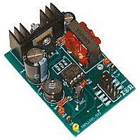
Manufacturer Part Number
IRPLLED1
Description
BOARD EVALUATION FOR IRS2540PBF
Manufacturer
International Rectifier
Specifications of IRPLLED1
Current - Output / Channel
1.5A
Outputs And Type
1, Non-Isolated
Voltage - Output
24V
Features
Dimmable
Voltage - Input
50 ~ 170V
Utilized Ic / Part
IRS2540PBF
Core Chip
IRS2540, IRS2541, IRS25401
Topology
Buck (Step Down)
No. Of Outputs
1
Output Current
1.5A
Output Voltage
500mV
Dimming Control Type
PWM
Development Tool Type
Hardware - Eval/Demo Board
Lead Free Status / RoHS Status
Contains lead / RoHS compliant by exemption


The overvoltage / open-circuit protection circuit shown in Figure 29 replaces schemes used on previous versions of
the IRPLLED1 reference design. This method offers far more reliable performance over the range of operating
conditions with or without an output capacitor. It also works reliably during PWM dimming.
The output over voltage / open circuit protection circuit shown in Figure 29 allows the designer to program the
allowable maximum output voltage by means of ROV1 and ROV2. An industry standard programmable zener diode
type LM431 (IC2) is used to pull down the base of Q1, which pulls down on VCC when the divided voltage from
ROV1 and ROV2 exceeds the internal 2.5V reference. IC2 is capable of sinking no more than 100mA and in the
SOT-23 package has limited power handling ability, therefore Q1 was added to pull down the VCC voltage fed from
RS1 and RS2 to below the under voltage lockout threshold VCCUV- of the IRS2540/1/01/11 causing it to
shutdown. This circuit reacts very rapidly when the output voltage exceeds the predetermined level. It operates
whether or not an output capacitor is connected, i.e. in any of the alternative JDIM jumper positions.
The over voltage protection threshold has been set to 32V in the IRPLLED1 Rev D demo board to allow one or two
standard LED panels to be connected in series to the output before reaching a voltage level high enough to trigger
the protection circuit. The open circuit protection circuit operates in hiccup mode such that Q1 pulls the VCC
voltage below the VCCUV- threshold causing the IRS2540/1/01/11 to switch off and enter micro power mode and
the output to fall to zero. VCC then charges up again through RS1 until the voltage again exceeds VCCUV+ and the
IRS2540/1/01/11 starts up again. The sequence then repeats until a load is added to clamp the output voltage.
The above circuit is able to limit the output voltage to a series of pulses instead of a DC level. However it should be
noted reducing the average output voltage does not prevent the possibility of electric shock in non-isolated
systems! Therefore an IRS2540/1/01/11 based Buck LED driver running directly off line would still be an electric
shock hazard and it would not be safe to attempt to replace the LEDs if such a system were powered. In non-isolated
systems, additional mechanical protection is required to ensure that access to the LEDs is not possible or alternative
a mechanical isolation system could be used to disconnect the LEDs completely from the ballast for safe access. In
an illuminated sign for example, this would be a reasonable approach.
The open circuit protection system described in this section can only be an effective safety feature in a system where
the IRS2540/1/01/11 Buck stage is used as a back end stage supplied by an already isolated DC source. It does
however serve to limit the output voltage to prevent damage to the output capacitor COUT in cases where the bus
voltage is greater than the rating of this capacitor.
Note:
The over voltage protection scheme used in the IRPLLED1 evaluation board is different to that used in earlier
revisions of the IRPLLED1 and does not conflict with the synchronization operation described in the previous
section.
The open load protection circuit in Fig 29 is recommended for isolated non-dimming applications where the load
may be disconnected and then reconnected without shutting down the driver. When the load is reconnected with
power on this would reduce the initial surge of current to the output reducing stress on the LEDs.
In an open circuit condition, switching will continue at the HO and LO outputs, whether due to the output voltage
clamp or to the watchdog timer.
Due to the operation of this circuit the output voltage under open circuit conditions where JDIM is in the DIM
position is made up of pulses as shown in Fig 30. If JDIM is in the REG position then these pulses will delay slowly
as the output discharges. This can leave an average voltage of approximately 50V at the output. The decay rate of
these pulses depends on the value of COUT and the interval between pulses depends on the time taken for CVCC1
to charge above VCCUV- through RS1 and therefore depends on the input voltage.
RD-0608
23
www.irf.com
Related parts for IRPLLED1
Image
Part Number
Description
Manufacturer
Datasheet
Request
R

Part Number:
Description:
SCHOTTKY RECTIFIER
Manufacturer:
International Rectifier Corp.
Datasheet:
Part Number:
Description:
SCHOTTKY RECTIFIER
Manufacturer:
International Rectifier Corp.
Datasheet:
Part Number:
Description:
SCHOTTKY RECTIFIER
Manufacturer:
International Rectifier Corp.
Datasheet:
Part Number:
Description:
SCHOTTKY RECTIFIER
Manufacturer:
International Rectifier Corp.
Datasheet:
Part Number:
Description:
SCHOTTKY RECTIFIER
Manufacturer:
International Rectifier Corp.
Datasheet:
Part Number:
Description:
SCHOTTKY RECTIFIER
Manufacturer:
International Rectifier Corp.
Datasheet:
Part Number:
Description:
SCHOTTKY RECTIFIER
Manufacturer:
International Rectifier Corp.
Datasheet:
Part Number:
Description:
SCHOTTKY RECTIFIER
Manufacturer:
International Rectifier Corp.
Datasheet:
Part Number:
Description:
SCHOTTKY RECTIFIER
Manufacturer:
International Rectifier Corp.
Datasheet:
Part Number:
Description:
SCHOTTKY RECTIFIER
Manufacturer:
International Rectifier Corp.
Datasheet:
Part Number:
Description:
SCHOTTKY RECTIFIER
Manufacturer:
International Rectifier Corp.
Datasheet:
Part Number:
Description:
SCHOTTKY RECTIFIER
Manufacturer:
International Rectifier Corp.
Datasheet:
Part Number:
Description:
SCHOTTKY RECTIFIER
Manufacturer:
International Rectifier Corp.
Datasheet:
Part Number:
Description:
SCHOTTKY RECTIFIER
Manufacturer:
International Rectifier Corp.
Datasheet:
Part Number:
Description:
SCHOTTKY RECTIFIER
Manufacturer:
International Rectifier Corp.
Datasheet: