NCP5603GEVB ON Semiconductor, NCP5603GEVB Datasheet - Page 2
NCP5603GEVB
Manufacturer Part Number
NCP5603GEVB
Description
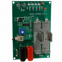
EVAL BOARD FOR NCP5603G HI FREQ
Manufacturer
ON Semiconductor
Specifications of NCP5603GEVB
Design Resources
NCP5603 EVB BOM NCP5603GEVB Gerber Files NCP5603 EVB Schematic
Current - Output / Channel
160mA
Outputs And Type
1, Non-Isolated
Voltage - Output
4.5 ~ 5 V
Features
Dimmable
Voltage - Input
3V or 3.6V
Utilized Ic / Part
NCP5603
Core Chip
NCP5603
Topology
Charge Pump
No. Of Outputs
1
Development Tool Type
Hardware - Eval/Demo Board
Leaded Process Compatible
Yes
Mcu Supported Families
NCP5603
Rohs Compliant
Yes
Lead Free Status / RoHS Status
Lead free / RoHS Compliant
For Use With/related Products
NCP5603G
Other names
NCP5603GEVBOS


it is worthwhile to note the thermal behavior of both the
silicon and the power LED.
(LWW5SG ) should have a maximum 4.5 V forward drop
with 350 mA current. The power absorbed by the load will
be 1.57 W and, assuming a 75% efficiency of the DC/DC
converter, will translate to almost 2 W of input power.
Consequently, some 400 mW will be dissipated as heat into
the silicon and, according to the NCP5603 data sheet, the
chip temperature will increase by R
34 DC. Such a temperature increase is acceptable since,
even under the worst case +85 C ambient temperature, the
junction will be below the maximum rating defined for this
chip.
situation: in this case, the efficiency of the converter can
decrease and we end up with 60% efficiency, yielding
almost 54 DC temperature increases. At this point, the
silicon can rise above 125 C, under extreme high ambient
temperature, and the global long−term reliability of the chip
will be impaired. This can be avoided by either reducing the
thermal resistance (using a heatsink by means of the PCB
layer) or by ensuring the duty cycle is short enough to
properly cool off the chip between pulses.
limited and care must be observed to avoid any thermal run
out during normal operation. This is particularly true for the
flash mode in which, as depicted above, nearly 1.6 W are
dissipated into the LED junctions. Because the junction to
ambient thermal resistance is limited by the packaging of the
Table 1. White LED Typical Applications
OSRAM LWY85S
OSRAM – LWT67C
OSRAM
OSRAM – LWW5SG
CITIZEN − CL590S
NICHIA−NECWB205
LUMILED
Along with the amount of current the converter provides,
According to the OSRAM’s data sheet, the Dragon LED
However, we must take into account the low battery
Generally speaking, the High Intensity LED are power
LED
qJA
x Pin = 85 x 0.4 =
1 mA – 10 mA
1 mA – 20 mA
1 mA – 20 mA
1 mA – 20 mA
Backlight
http://onsemi.com
AND8192/D
2
LED, a good thermal contact to a dedicated layer on the
printed board is essential. The LWW5SG specifications give
a maximum 9 C/W junction−to−case thermal resistance,
capable of limiting the temperature of the silicon to the
100 C maximum specified in the OSRAM data sheet. After
dissipating 1.6 W, the maximum thermal to air resistance
acceptable by the chip can be calculated as:
achieve a 0.38 C/W case to ambient thermal resistance and
the only alternative is to limit the operating ambient
temperature.
25 C/W.
25 − 9 = 16 C/W, a value more realistic, although not so easy
to achieve with a room limited PCB.
thermal sinking and a simple copper flag is built underneath
the QFN package as depicted Figure 3.
illustrates the three functions:
Since the R
Assuming T
In this case, the case−to−ambient thermal resistance is
NCP5603 operates without special treatment in terms of
The schematic of the multiple application, Figure 2,
Backlight³ four LED in parallel, dimming capability.
Torch
Flash
100 mA
Torch
³ one LED, no output adjustment.
³ one power LED, pulse width adjustable.
R qJA +
qJC
amb
R qJA +
is 9 C/W, it is practically impossible to
= 60 C, then R
100 * 85
1.6
T jmax * T amb
P chip
+ 9.37°C W
qJA
= (100−60) / 1.6 =
350 mA
800 mA
Flash
Related parts for NCP5603GEVB
Image
Part Number
Description
Manufacturer
Datasheet
Request
R

Part Number:
Description:
High Efficiency Charge Pump Converter
Manufacturer:
ON Semiconductor
Datasheet:
Part Number:
Description:
ON Semiconductor [VOLTAGE REGULATOR]
Manufacturer:
ON Semiconductor
Datasheet:
Part Number:
Description:
357-036-542-201 CARDEDGE 36POS DL .156 BLK LOPRO
Manufacturer:
ON Semiconductor
Datasheet:
Part Number:
Description:
357-036-542-201 CARDEDGE 36POS DL .156 BLK LOPRO
Manufacturer:
ON Semiconductor
Datasheet:
Part Number:
Description:
357-036-542-201 CARDEDGE 36POS DL .156 BLK LOPRO
Manufacturer:
ON Semiconductor
Datasheet:
Part Number:
Description:
357-036-542-201 CARDEDGE 36POS DL .156 BLK LOPRO
Manufacturer:
ON Semiconductor
Datasheet:
Part Number:
Description:
357-036-542-201 CARDEDGE 36POS DL .156 BLK LOPRO
Manufacturer:
ON Semiconductor
Datasheet:
Part Number:
Description:
357-036-542-201 CARDEDGE 36POS DL .156 BLK LOPRO
Manufacturer:
ON Semiconductor
Datasheet:
Part Number:
Description:
357-036-542-201 CARDEDGE 36POS DL .156 BLK LOPRO
Manufacturer:
ON Semiconductor
Datasheet:
Part Number:
Description:
357-036-542-201 CARDEDGE 36POS DL .156 BLK LOPRO
Manufacturer:
ON Semiconductor
Datasheet:
Part Number:
Description:
357-036-542-201 CARDEDGE 36POS DL .156 BLK LOPRO
Manufacturer:
ON Semiconductor
Datasheet:
Part Number:
Description:
357-036-542-201 CARDEDGE 36POS DL .156 BLK LOPRO
Manufacturer:
ON Semiconductor
Datasheet:
Part Number:
Description:
Manufacturer:
ON Semiconductor
Datasheet:
Part Number:
Description:
Manufacturer:
ON Semiconductor
Datasheet: