MCP6V01RD-TCPL Microchip Technology, MCP6V01RD-TCPL Datasheet - Page 5
MCP6V01RD-TCPL
Manufacturer Part Number
MCP6V01RD-TCPL
Description
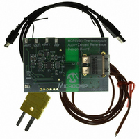
REF DESIGN THERMCPL FOR MCP6V01
Manufacturer
Microchip Technology
Datasheets
1.MCP6V01RD-TCPL.pdf
(44 pages)
2.MCP6V01RD-TCPL.pdf
(30 pages)
3.MCP6V03-ESN.pdf
(40 pages)
Specifications of MCP6V01RD-TCPL
Channels Per Ic
1 - Single
Amplifier Type
Chopper (Zero-Drift)
Output Type
Rail-to-Rail
Slew Rate
0.5 V/µs
Current - Output / Channel
22mA
Operating Temperature
-40°C ~ 125°C
Voltage - Supply, Single/dual (±)
1.8 V ~ 5.5 V
Board Type
Fully Populated
Utilized Ic / Part
MCP6V01
Silicon Manufacturer
Microchip
Silicon Core Number
MCP6V01
Kit Application Type
Sensing - Temperature
Application Sub Type
Temperature Sensor
Processor To Be Evaluated
MCP6V01
Lead Free Status / RoHS Status
Lead free / RoHS Compliant
-3db Bandwidth
-
Current - Supply (main Ic)
-
Lead Free Status / Rohs Status
Lead free / RoHS Compliant


1.3
FIGURE 1-1:
FIGURE 1-2:
Time.
FIGURE 1-3:
FIGURE 1-4:
© 2008 Microchip Technology Inc.
V
V
OUT
V
V
V
CS
I
I
I
V
OUT
DD
CS
SS
V
OS
DD
OS
IN
IN
1 µA
(typical)
-2 µA
(typical)
V
(typical)
Timing Diagrams
V
0V
DD
DD
High-Z
/5 MΩ
t
t
ODR
ON
1.8V
t
t
V
STL
STR
IL
Amplifier Start Up.
Offset Correction Settling
V
Output Overdrive Recovery.
Chip Select (MCP6V03).
DD
(typical)
(typical)
(typical)
/2
300 µA
300 µA
5 pA
V
SS
V
t
ODR
V
IH
1.8V to 5.5V
V
V
V
OS
OS
OS
OS
t
OFF
V
+ 50 µV
– 50 µV
+ 50 µV
+ 50 µV
DD
(typical)
(typical)
(typical)
High-Z
/5 MΩ
-2 µA
1 µA
1.4
The circuits used for the DC and AC tests are shown in
Figure 1-5
out as discussed in Section 4.3.7 “Supply Bypassing
and Filtering”. R
of R
FIGURE 1-5:
Most Non-Inverting Gain Conditions.
FIGURE 1-6:
Most Inverting Gain Conditions.
The circuit in
dynamic behavior (i.e., IMD, t
potentiometer balances the resistor network (V
should equal V
mode input voltage is V
input (V
10 V/V.
FIGURE 1-7:
Input Behavior.
V
V
V
V
V
DD
DD
IN
F
IN
IN
MCP6V0X
MCP6V0X
and R
/3
/3
20.0 kΩ
20.0 kΩ
ERR
0.1%
0.1%
Test Circuits
R
R
R
R
G
G
N
N
and
G
) appears at V
to minimize bias current effects.
Figure
Figure 1-7
REF
20.0 kΩ
MCP6V0X
20.0 kΩ
N
0.1%
0.1%
V
V
V
DD
DD
DD
is equal to the parallel combination
MCP6V01/2/3
at DC). The op amp’s common
AC and DC Test Circuit for
AC and DC Test Circuit for
Test Circuit for Dynamic
1-6. Lay the bypass capacitors
100 nF
100 nF
100 nF
1 µF
CM
R
R
25 turn
24.9 Ω
1 µF
1 µF
50Ω
F
F
tests the op amp input’s
OUT
= V
STR
IN
R
R
with a noise gain of
, t
/2. The error at the
ISO
ISO
R
STL
C
C
ISO
L
L
C
DS22058B-page 5
and t
L
V
REF
R
R
L
L
ODR
V
V
V
L
L
L
V
V
V
R
). The
OUT
OUT
OUT
L
OUT
Related parts for MCP6V01RD-TCPL
Image
Part Number
Description
Manufacturer
Datasheet
Request
R

Part Number:
Description:
Manufacturer:
Microchip Technology Inc.
Datasheet:
Part Number:
Description:
Manufacturer:
Microchip Technology Inc.
Datasheet:
Part Number:
Description:
Manufacturer:
Microchip Technology Inc.
Datasheet:
Part Number:
Description:
Manufacturer:
Microchip Technology Inc.
Datasheet:
Part Number:
Description:
Manufacturer:
Microchip Technology Inc.
Datasheet:
Part Number:
Description:
Manufacturer:
Microchip Technology Inc.
Datasheet:
Part Number:
Description:
Manufacturer:
Microchip Technology Inc.
Datasheet:
Part Number:
Description:
Manufacturer:
Microchip Technology Inc.
Datasheet: