AD8260-EVALZ Analog Devices Inc, AD8260-EVALZ Datasheet - Page 20
AD8260-EVALZ
Manufacturer Part Number
AD8260-EVALZ
Description
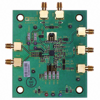
BOARD EVAL FOR AD8260
Manufacturer
Analog Devices Inc
Specifications of AD8260-EVALZ
Channels Per Ic
1 - Single
Amplifier Type
Variable Gain
Output Type
Differential
Slew Rate
730 V/µs
-3db Bandwidth
195MHz
Current - Output / Channel
310mA
Operating Temperature
-40°C ~ 105°C
Current - Supply (main Ic)
28.3mA
Voltage - Supply, Single/dual (±)
3.3 V ~ 10 V, ±3.3 V ~ 5 V
Board Type
Fully Populated
Utilized Ic / Part
AD8260
Silicon Manufacturer
Analog Devices
Application Sub Type
Programmable Gain Amplifier
Kit Application Type
Amplifier
Silicon Core Number
AD8260
Kit Contents
Board
Lead Free Status / RoHS Status
Lead free / RoHS Compliant
Lead Free Status / RoHS Status
Lead free / RoHS Compliant, Lead free / RoHS Compliant


AD8260
THEORY OF OPERATION
OVERVIEW
The AD8260 is a self-contained transceiver intended for analog
communications using a power line as the media. Operating on
supplies as low as 3.3 V, it includes a high current driver usable
as a transmitter and a low noise digitally programmable variable
gain amplifier (DGA), usable as a receiver (see Figure 64). An
uncommitted current-feedback high frequency op amp acts as a
preamplifier and interface to the DGA and is user configured
for gains greater than 6 dB. Combined, the VGA and preamplifier
are usable at high signal levels from dc to 100 MHz, with a
small-signal −3 dB bandwidth of 230 MHz. To implement a
high current-output VGA, the VGA output can be connected
to the driver-amplifier differential input.
The small-signal −3 dB bandwidth of the driver amplifier is
195 MHz and the large-signal bandwidth is >115 MHz, even
when driving a 50 Ω load.
The device is fabricated on the Analog Devices, Inc., high speed
(eXtra Fast Complementary Bipolar) XFCB process. The pream-
plifier and DGA feature low dc offset voltage, and a nominal
gain range of −6 dB to +24 dB, a 30 dB gain span, and a differential
output for ADC driving. The power consumption is 93 mW
with a single 3.3 V supply. The supply current is typically about
28 mA when all circuits in the device are active. During normal
usage, either the driver amplifier is on or the preamplifier and
DGA are on and, therefore, the supply current in general is less
than 28 mA. The gain of the AD8260 VGA is programmed via a
Rev. 0 | Page 20 of 32
4-bit parallel interface. Figure 64 shows the circuit block
diagram and basic application connections, and illustrates the
envisioned external DAC, ADC, and power-line bus interface
connections. The diagram shows the connections for single 3.3 V
supply operation; if a dual supply is available, the VMID
generator can be shut down and Pin VMDI, Pin VMDO, and
Pin VOCM need to be grounded. Note that Pin VNCM
functions as the negative supply for the bias and VMID cells,
plus the logic interfaces, and should always be tied to ground.
For optimal dynamic range, it is important that the inputs and
outputs to both the driver amplifier and the preamplifier and
the DGA output amplifier be ac-coupled in a single-supply
application. In Figure 64, the DAC and ADC are presumed to
operate on a 1.8 V or 3.3 V supply with a corresponding limited
output and input swing. The DAC outputs are currents that
point down and generate a voltage in the 50 Ω resistors that are
connected to ground. The maximum voltage with a peak DAC
output current of 15 mA is 0.75 V; if a DAC with a 20 mA peak
current is used, then the maximum voltage is 1 V per side for a
differential input signal of 2 V p-p.
The driver amplifier supports a 3 V p-p output swing on a
3.3 V supply. Because of its gain of 1.5, the maximum input
swing is 2 V p-p. The corresponding maximum output swing for
the DGA is 2.4 V p-p differential; the input to the preamplifier
can be a maximum of 0.6 V p-p.
Related parts for AD8260-EVALZ
Image
Part Number
Description
Manufacturer
Datasheet
Request
R

Part Number:
Description:
High Speed, Low Power Dual Operational Amplifier
Manufacturer:
Analog Devices
Datasheet:

Part Number:
Description:
±1.7g Dual-Axis IMEMS Accelerometer Evaluation Board
Manufacturer:
Analog Devices Inc
Datasheet:

Part Number:
Description:
Inertial Sensor Evaluation System
Manufacturer:
Analog Devices Inc
Datasheet:
Part Number:
Description:
Manufacturer:
Analog Devices Inc
Datasheet:
Part Number:
Description:
Manufacturer:
Analog Devices Inc
Datasheet:
Part Number:
Description:
Manufacturer:
Analog Devices Inc
Datasheet:
Part Number:
Description:
Manufacturer:
Analog Devices Inc
Datasheet:
Part Number:
Description:
Manufacturer:
Analog Devices Inc
Datasheet:
Part Number:
Description:
Manufacturer:
Analog Devices Inc
Datasheet:
Part Number:
Description:
Manufacturer:
Analog Devices Inc
Datasheet:
Part Number:
Description:
Manufacturer:
Analog Devices Inc
Datasheet:
Part Number:
Description:
Manufacturer:
Analog Devices Inc
Datasheet:
Part Number:
Description:
Manufacturer:
Analog Devices Inc
Datasheet: