AD8260-EVALZ Analog Devices Inc, AD8260-EVALZ Datasheet - Page 27
AD8260-EVALZ
Manufacturer Part Number
AD8260-EVALZ
Description
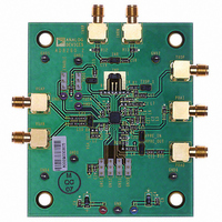
BOARD EVAL FOR AD8260
Manufacturer
Analog Devices Inc
Specifications of AD8260-EVALZ
Channels Per Ic
1 - Single
Amplifier Type
Variable Gain
Output Type
Differential
Slew Rate
730 V/µs
-3db Bandwidth
195MHz
Current - Output / Channel
310mA
Operating Temperature
-40°C ~ 105°C
Current - Supply (main Ic)
28.3mA
Voltage - Supply, Single/dual (±)
3.3 V ~ 10 V, ±3.3 V ~ 5 V
Board Type
Fully Populated
Utilized Ic / Part
AD8260
Silicon Manufacturer
Analog Devices
Application Sub Type
Programmable Gain Amplifier
Kit Application Type
Amplifier
Silicon Core Number
AD8260
Kit Contents
Board
Lead Free Status / RoHS Status
Lead free / RoHS Compliant
Lead Free Status / RoHS Status
Lead free / RoHS Compliant, Lead free / RoHS Compliant


CONNECTING THE EVALUATION BOARD
Figure 69 shows an evaluation board with typical test connec-
tions. The various pieces of test equipment are representative,
and equivalent equipment may be substituted.
The AD8260 includes two amplifier channels: a high current
driver and a digitally controlled VGA that is independently
enabled. The slide switch labeled ENABLE functions as the chip
enable, the GNSx switches permit the preamplifier/VGA to
operate, and the TX_EN switch enables the high current driver.
These independent enable functions permit the device to
operate in a send or listen mode when used as a transceiver.
The high current driver features differential inputs and is
optimally driven by a differential signal source. The input signal
is monitored at the 2-pin header labeled INP, using a differential
probe such as the Tektronix P6247 (not shown). Two 49.9 Ω
resistors are provided (R12 and R13), either for terminating
coaxial cables from a signal generator or to be used as load
resistors for a DAC with a current source output. An optional
external load resistor is connected at the SMA connector TXOP
and the output signal monitored at the 2-pin header labeled
TXOP_1.
As shipped, the gain of the high current driver is 1.5×, its default
value. The internal differential network with resistor values of
1 kΩ and 1.5 kΩ establishes this value. Other values of gain are
realized by connecting external resistors to the device at Pin 23,
Pin 24, Pin 27, Pin 28, and Pin 31, as shown in Figure 68, which
shows the internal structure for the default gain and how the
gain can be modified.
Rev. A | Page 27 of 32
The VGA/preamplifier is completely independent of the high
current driver and features a single-ended input at the SMA
connector PRAI. The input signal is monitored at the header
VPRE_IN. The output is monitored at the 2-pin header
VGA_OUT.
The gain bits, GNS0 through GNS3, must be set before the
VGA/preamplifier can operate. Table 4 lists the binary gain
codes. The board is shipped with both enables (ENBL and
TXEN) engaged and the gain-code switches adjusted for
maximum DGA gain (1011). Resistor R5 and Resistor R6
establish the preamplifier gain and are 100 Ω as shipped for a
noninverting preamplifier gain of 2×.
Figure 68. Gain-Setting Resistors of the High Current Driver
VOCM
INRN
INPP
INRP
INPN
COMPONENTS ARE SHOWN IN BLACK,
32
31
30
29
28
OPTIONAL COMPONENTS
DEFAULT GAIN SETTING
ARE SHOWN IN GRAY.
1.5kΩ
1kΩ
1kΩ
1
VMDO
C COMP
+
–
1.5kΩ
24
23
27
AD8260
TXFB
TXOP
TXOP
Related parts for AD8260-EVALZ
Image
Part Number
Description
Manufacturer
Datasheet
Request
R

Part Number:
Description:
High Speed, Low Power Dual Operational Amplifier
Manufacturer:
Analog Devices
Datasheet:

Part Number:
Description:
±1.7g Dual-Axis IMEMS Accelerometer Evaluation Board
Manufacturer:
Analog Devices Inc
Datasheet:

Part Number:
Description:
Inertial Sensor Evaluation System
Manufacturer:
Analog Devices Inc
Datasheet:
Part Number:
Description:
Manufacturer:
Analog Devices Inc
Datasheet:
Part Number:
Description:
Manufacturer:
Analog Devices Inc
Datasheet:
Part Number:
Description:
Manufacturer:
Analog Devices Inc
Datasheet:
Part Number:
Description:
Manufacturer:
Analog Devices Inc
Datasheet:
Part Number:
Description:
Manufacturer:
Analog Devices Inc
Datasheet:
Part Number:
Description:
Manufacturer:
Analog Devices Inc
Datasheet:
Part Number:
Description:
Manufacturer:
Analog Devices Inc
Datasheet:
Part Number:
Description:
Manufacturer:
Analog Devices Inc
Datasheet:
Part Number:
Description:
Manufacturer:
Analog Devices Inc
Datasheet:
Part Number:
Description:
Manufacturer:
Analog Devices Inc
Datasheet: