ATSAM3U-EK Atmel, ATSAM3U-EK Datasheet
ATSAM3U-EK
Specifications of ATSAM3U-EK
Available stocks


Related parts for ATSAM3U-EK


ATSAM3U-EK Summary of contents
Page 1
SAM3U-EK Evaluation Kit .................................................................................................................... User Guide 6478E–ATARM–30-Mar-11 ...
Page 2
Section 1 Introduction .................................................................................................................1-1 1.1 SAM3U Evaluation Kit........................................................................................................ 1-1 1.2 User Guide ......................................................................................................................... 1-1 1.3 References and Applicable Documents ............................................................................. 1-1 Section 2 Kit Contents ................................................................................................................2-1 2.1 Deliverables ....................................................................................................................... 2-1 2.2 Electrostatic Warning ......................................................................................................... 2-2 Section 3 Power Up ....................................................................................................................3-1 ...
Page 3
ZigBee ............................................................................................................... 4-17 4.3.19 PIO Expansion ................................................................................................... 4-18 4.4 Configuration.................................................................................................................... 4-19 4.4.1 PIO Usage ......................................................................................................... 4-19 4.4.2 Jumpers ............................................................................................................. 4-22 4.4.3 Test Points ......................................................................................................... 4-23 4.4.4 Solder Drops ...................................................................................................... 4-23 4.4.5 Assigned PIO Lines, Disconnection Possibility.................................................. 4-23 Section 5 ...
Page 4
... Section 4 describes the hardware resources, and includes default jumper and switch settings, and the schematics. Section 5 provides all the board schematics Section 6 give troubleshooting recommendations 1.3 References and Applicable Documents Table 1-1. References and Applicable Documents SAM3U Datasheet SAM3U-EK Evaluation Kit User Guide Title http://www.atmel.com/dyn/products/product_card.asp?part_id=4562 Section 1 Introduction Comment 6478E–ATARM–30-Mar-11 1-1 ...
Page 5
... USB cable one serial RS232 cable A Welcome Letter Figure 2-1. Unpacked SAM3U-EK Unpack and inspect the kit carefully. Contact your local Atmel distributor, should you have issues con- cerning the contents of the kit. SAM3U-EK Evaluation Kit User Guide Section 2 Kit Contents 2-1 6478E– ...
Page 6
Kit Contents 2.2 Electrostatic Warning The SAM3U-EK board is shipped in a protective anti-static package. The board must not be subjected to high electrostatic potentials. A grounding strap or similar protective device should be worn when han- dling the board. ...
Page 7
... Recovery Procedure The DevStart ends by giving step-by-step instructions on how to recover the SAM3U-EK to the state as it was when shipped by Atmel. Follow the instructions if you deleted the contents of the embedded Flash or the NAND Flash and want to recover from this situation. SAM3U-EK Evaluation Kit User Guide ...
Page 8
... Power Up 3.5 Sample Code and Technical Support After boot up, you can run some sample code or your own application on the development kit. You can http://www.atmel.com/products/at91/sam3landing.asp?family_id=605 Figure 3-1. Atmel Website for SAM3U Series 3-2 6478E–ATARM–30-Mar- SAM3U-EK Evaluation Kit User Guide ...
Page 9
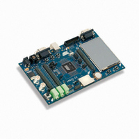
... Board Overview This section introduces the Atmel SAM3U Evaluation Kit design. It introduces system-level concepts, such as power distribution, memory, and interface assignments. The SAM3U-EK board is based on the integration of an ARM PSRAM (pseudo-static RAM), NAND Flash and a set of popular peripherals designed to provide a high performance processor evaluation solution with high flexibility for various kinds of applications ...
Page 10
Evaluation Kit Hardware 4.2 Features List Here is the list of the main board components and interfaces: SAM3U4E QFP chip with optional socket footprint 12 MHz crystal 32.768 KHz crystal Optional SMB connector, for external system clock input PSRAM NAND ...
Page 11
The SAM3U4E features an External Bus Interface (EBI) that permits interfacing to a broad range of external memories and virtually to any parallel peripheral. The SAM3U-EK board is equipped with two kinds of memory devices connected to the SAM3U4E EBI: ...
Page 12
Evaluation Kit Hardware Figure 4-3. NAND Flash P B [31:0] NANDRDY NANDOE P C [31:0] NCS1 NANDCL E NANDAL E NANDW E +3V 3 The chip select signals NCS0 and NCS1 are used for PSRAM and NAND ...
Page 13
Figure 4-4. External Clock Source XIN32 XOUT 32 XIN XOUT 4.3.4 Reset and Wake-Up Circuitry The on-board NRST button BP1 and NRSTB button BP2 provide the SAM3U4E with external reset con- trol. The on-board WAKE-UP button BP3 can be used ...
Page 14
Evaluation Kit Hardware The FWUP pin is Force Wake-Up active low input enabled as a wake-up source with external pull- up. If the FWUP pin is asserted for a time longer than the debouncing period (configurable for 100 ...
Page 15
Figure 4-7. Backup Battery MN1B MN1B S AM3U S AM3U 4.3.6 UART The Universal Asynchronous Receiver Transmitter features a two-pin UART that can be used for com- munication and trace purposes. It offers an ideal channel for in-situ programming solutions. ...
Page 16
Evaluation Kit Hardware Figure 4-9. USART + A[31:0] 100K 100K TXD1 P A20 RXD1 P A21 RTS1 P A22 CTS1 P A23 ...
Page 17
Table 4-1. LCD Module Pin Out Pin 6~21 22~ 33~36 37~38 39 The LCD module gets its reset from NRST. As explained previously, this NRST is ...
Page 18
Evaluation Kit Hardware Figure 4-11. LCD Block P B [31: ...
Page 19
Figure 4-12. Touch Screen Controller X_R _UP X_LE _DOW N MN5 MN5 ADS 7843E ADS 7843E X_R _UP X_LE _DOW N ...
Page 20
Evaluation Kit Hardware The SAM3U4E programmable clock output is used to generate the WM8731 master clock (MCLK). The SAM3U4E ODT (On-Die Termination) feature guarantees a signal integrity on this clock line without the need for external discrete components. WM8731 pin ...
Page 21
Figure 4-15. Codec Block MN8 MN8 + M8731E DS XW M8731E 10uF 10uF 100nF 100nF 100nF 100nF ...
Page 22
... There are 8 multiplexed analog channel inputs on the 12-bit ADC, and 8 multiplexed analog channel inputs on the 10-bit ADC. SAM3U-EK optionally connects the two ADC channels to BNC header (check for your actual components implementation, schematics and BOM, on http://www.atmel.com/products/). One is 12-bit ADC channel 3, shared with PIO pin PB4. The other one is 10-bit ADC channel 0, shared with PIO PB5 ...
Page 23
Figure 4-18. User Buttons 4.3.15 G-Sensor The SAM3U-EK board is equipped with a three axis accelerometer MMA7341. Basically acceler- ation to analog voltage converter. Converted data on corresponding directions are read by 3 SAM3U4E 12-bit ADC channels. ...
Page 24
Evaluation Kit Hardware Figure 4-19. G-Sensor P B [31: [31:0] 3AXS_SL ADC0_AD2 ADC0_AD6 ADC0_AD7 4.3.16 Temperature Sensor A temperature sensor MCP9800 is connected to ...
Page 25
Figure 4-21. SD Card Socket P A[31: [31:0] DA2 P A7 DA3 P A8 DA4 CDA DA5 DA6 DA7 W KUP12 P A25 P ...
Page 26
Evaluation Kit Hardware 4.3.19 PIO Expansion Figure 4-23. PIO Expansion Ports P B [31: [31:0] + 048 048 ...
Page 27
Configuration This section describes the PIO usage, the jumpers, the test points and the solder drops of a SAM3U-EK board. 4.4.1 PIO Usage Table 4-5. PIO Port A Assignment I/O Line Peripheral A PA0 TIOB0 PA1 TIOA0 PA2 TCLK0 ...
Page 28
Evaluation Kit Hardware Table 4-5. PIO Port A Assignment I/O Line Peripheral A PA29 RK PA30 TF PA31 RF Table 4-6. PIO Port B Assignment I/O Line Peripheral A PB0 PWMH0 PB1 PWMH1 PB2 PWMH2 PB3 PWMH3 PB4 TCLK1 PB5 ...
Page 29
Table 4-6. PIO Port B Assignment I/O Line Peripheral A PB29 D12 PB30 D13 PB31 D14 Table 4-7. PIO Port C Assignment I/O Line Peripheral A PC0 A2 PC1 A3 PC2 A4 PC3 A5 PC4 A6 PC5 A7 PC6 A8 ...
Page 30
Evaluation Kit Hardware Table 4-7. PIO Port C Assignment I/O Line Peripheral A PC29 PWML0 PC30 PWML1 PC31 PWML2 4.4.2 Jumpers The SAM3U-EK board jumpers are used for many purposes such as internal Flash Memory reinitializa- tion, power current measurement ...
Page 31
Test Points Some test points have been placed on the SAM3U-EK board for the verification of important signals. Table 4-9. Test Points Designation TP1 TP2 TP3 TP4 TP5 TP6 TP7 TP8 TP9 TP10 TP11 TP12 TP13 TP14 TP15 TP16 ...
Page 32
Evaluation Kit Hardware tors, for example). This feature gives the user an added level of versatility for prototyping a system of his own. See the table below. Table 4-11. Disconnecting Possibility Designation R14 R15 R16 R20 R24 R25 R26 R46 ...
Page 33
Schematics This section contains the following schematics: Block Diagram Design Notes SAM3U PIO SAM3U CPU EBI Memory 1MB PSRAM EBI Memory II 2GB NAND Flash TFT LCD and TSC UART and COM1 RS232 Audio DAC SD/MMC Interface Accelerometer, Temp, ...
Page 34
... D ATMEL Cortex M3 Processor SAM3U (LQFP144) Reset,Debug Logic C Audio DAC Accelerometer Temperature sense B USB & UART SAM3U-EK RevB Block Diagram User Interface (PIO PortA,B, Power Manage SD/MMC Card PSRAM Nand Flash 2.8 Inch TFT-LCD ZXL ZXL ZXL 19-MAY-09 19-MAY-09 19-MAY- INIT EDIT ...
Page 35
D 1. SAM3U-EK Revision HISTORY C 2. Explain of Schematics Rev: A SCH: SAM3U-EK RevA Data: 2008/12 Note: Original Released Rev: B SCH: SAM3U-EK RevB Data: 2009/04 Note: Final Released (1) Resistance Unit: "K" ...
Page 36
PA[31: {5,6,7,10,11,14,15} PC[31: MN1A MN1A SAM3U SAM3U PA0 109 PA0/WKUP0 PA1 111 PA1/WKUP1 PA2 113 PA2/WKUP2 PA3 115 PA3/CK PA4 117 PA4/CDA PA5 119 PA5/DA0 121 PA6 PA6/DA1 PA7 123 PA7/DA2 ...
Page 37
VIO +3V3 C106 C106 10nF 10nF R1 R1 {14} ERASE {14} TEST {14} JTAGSEL D {11,14} FWUP {13,14} SHDN VBG {14} VBG {7,11,12,14} NRST {11,14} NRSTB {12,14} TDI {12,14} TDO {12,14} TMS {12,14} TCK {12,14} DHSDP {12,14} DHSDM R2 ...
Page 38
D {3,6,7,11,13,14,15} PB[31:0] {3,6,7,10,11,14,15} PC[31:0] C JP12 JP12 JP JP PB20 NCS0 PB19 NRD PB23 NWE PB7 PB19 PB20 PB23 MN2 MN2 PSRAM 512K x16 PSRAM 512K x16 PB8 PC0 4 ...
Page 39
D {3,5,7,11,13,14,15} PB[31:0] C {3,5,7,10,11,14,15} PC[31:0] NCS1 +3V3 +3V3 R12 R12 R13 R13 4 47K 47K 47K 47K 5 6 PB24 R14 R14 NANDRDY PB17 8 NANDOE 9 ...
Page 40
PB[31:0] D {4,11,12,14} NRST C +3V3 + + C38 C38 C39 C39 10uF 10uF 100nF 100nF DGND {3,5,6,10,11,14,15} PC[31:0] B X_RIGHT Y_UP X_LEFT Y_DOWN TP1 TP1 SMD SMD A R28 R28 100K 100K AGND1 ...
Page 41
D {3,7,9,10,11,12,14,15} PA[31:0] PA12 UTXD PA11 URXD C B TXD1 PA20 RXD1 PA21 RTS1 PA22 PA23 CTS1 MN6 MN6 MAX3232CSE MAX3232CSE +3V3 16 VCC C1+ C44 C44 100nF 100nF 2 V+ C1- +3V3 +3V3 C46 ...
Page 42
C54 C54 C55 C55 C56 C56 10uF 10uF 100nF 100nF 100nF 100nF DGND + + C61 C61 C62 C62 10uF 10uF 100nF 100nF AGND +3V3 +3V3 +3V3 C R38 R38 R39 R39 R40 R40 100K ...
Page 43
D {3,7,8,9,11,12,14,15} PA[31:0] {3,5,6,7,11,14,15} PC[31:0] DA2 DA3 DA4 PC28 C CDA PC29 DA5 CK DA6 PC30 DA7 WKUP12 PC31 DA0 DA1 R56 R56 R57 R57 R58 R58 RA1 RA1 10K 10K 10K 10K 10K ...
Page 44
PB[31:0] D {3,5,6,7,10,14,15} PC[31:0] 3AXS_SLEEP# ADC0_AD2 ADC0_AD6 ADC0_AD7 C {3,7,8,9,10,12,14,15} PA[31:0] TWD0 TWCK0 TEMP_ALARM B {4,7,12,14} NRST {4,14} NRSTB WAKE_UP# {4,14} FWUP +3V3 +3V3 R59 R59 R60 R60 10K 10K 10K 10K JP15 JP15 ...
Page 45
D {4,14} DHSDP {4,14} DHSDM {3,7,8,9,10,11,14,15} PA[31:0] PA0 VBUS_USB C B {4,14} TDI {4,14} TMS {4,14} TCK {4,14} TDO {4,7,11,14} NRST R68 R68 47K 47K C88 C88 MN11 MN11 R69 R69 10pF 10pF TPD3E001DRLR TPD3E001DRLR ...
Page 46
J11 J11 MN13 MN13 MP179P 2.1mm MP179P 2.1mm ZEN056V130A24LS ZEN056V130A24LS R80 R80 IRLML2502 IRLML2502 10K 10K {4,14} SHDN C {3,5,6,7,11,14,15} PB[31:0] PB4 PB5 PB0 USR_LED1# USR_LED2# PB1 PB2 POWER_LED IRLML2502 ...
Page 47
D {3,7,8,9,10,11,12,15} PA[31:0] {3,5,6,7,11,13,15} PB[31:0] {3,5,6,7,10,11,15} PC[31:0] PC0 PB0 PC1 PB1 PC2 PB2 PC3 PB3 PC4 PB4 PC5 PB5 PC6 PB6 PC7 PB7 PC8 PB8 PC9 PB9 PC10 PB10 PC11 PB11 PC12 PB12 PC13 PB13 PC14 PB14 PC15 PB15 ...
Page 48
D {3,7,8,9,10,11,12,14} PA[31:0] {3,5,6,7,11,13,14} PB[31:0] {3,5,6,7,10,11,14} PC[31:0] +5V PC0 PC1 PC2 PC3 C PC4 PC5 PC6 PC7 PC8 PC9 PC10 PC11 PC12 PC13 PC14 PC15 +3V3 DGND B ZB_RSTN IRQ1_ZBEE SPIO_NPCS0# MISO SOLDER DROP 2 ...
Page 49
... Self-Test A test package software is available to implement a functional test for each section of the board. Refer to the SAM3U-EK page on www.atmel.com. 6.2 Board Recovery The SAM3U-EK is delivered with an on-board recovery procedure allowing to reprogram the board as it was when shipped. This procedure is accessible from the Flash disk mounted when the board is ...
Page 50
Troubleshooting 6-2 6478E–ATARM–30-Mar-11 SAM3U-EK Evaluation Kit User Guide ...
Page 51
JTAG/ICE: Missing Pull-up Resistor on TDO Pin The TDO pin is in input mode with the pull-up resistor disabled when the Cortex M3 is not in debug mode. Problem Fix/Workaround To avoid current consumption on VDDIO and/or VDDCORE due ...
Page 52
Revision History Table 8-1. Document Comments 6478E Erratum added as a Table 4-5, “PIO Port A Assignment” 6478D Vendor name and reference removed from PSRAM in 6478C Figure 4-2, ” PSRAM” Table 4-8 , JP15 and JP16 Default Settings ...
Page 53
... Disclaimer: The information in this document is provided in connection with Atmel products. No license, express or implied, by estoppel or otherwise, to any intellectual property right is granted by this document or in connection with the sale of Atmel products. EXCEPT AS SET FORTH IN ATMEL’S TERMS AND CONDI- TIONS OF SALE LOCATED ON ATMEL’S WEB SITE, ATMEL ASSUMES NO LIABILITY WHATSOEVER AND DISCLAIMS ANY EXPRESS, IMPLIED OR STATUTORY WARRANTY RELATING TO ITS PRODUCTS INCLUDING, BUT NOT LIMITED TO, THE IMPLIED WARRANTY OF MERCHANTABILITY, FITNESS FOR A PARTICULAR PURPOSE, OR NON-INFRINGEMENT ...