CT-161-CD Fujitsu Semiconductor America Inc, CT-161-CD Datasheet - Page 56
CT-161-CD
Manufacturer Part Number
CT-161-CD
Description
KIT 16LX FOR MB90F387
Manufacturer
Fujitsu Semiconductor America Inc
Series
F²MC-16LXr
Type
MCUr
Specifications of CT-161-CD
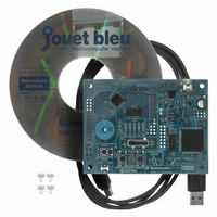
Contents
Board, Cable, CD
For Use With/related Products
MB90F387S
Lead Free Status / RoHS Status
Lead free / RoHS Compliant
Other names
865-1103
Available stocks
Company
Part Number
Manufacturer
Quantity
Price
Company:

Part Number:
CT-161-CD
Manufacturer:
Fujitsu Semiconductor America
Quantity:
135


The change of pin status can be detected by a program running on the microcomputer The
microcomputer of the Starter Kit can determine the status of pins P25 and P27 from the
corresponding values in an I-O port register (PDR2). Register values can be read using
instructions of a microcomputer program. In other words, the microcomputer can determine
the operation state of a switch by reading the corresponding value from PDR2 by the program.
Let us explain some specifications of PDR2. PDR2 is the 8-bit register that indicates the
status of port 2 pins (P20 to P27). Figure 3.3 shows the association of the pins at port 2 with
the bits of PDR2. When a pin is at the high level, the corresponding bit is 1; when the pin is
at the low level, the bit is 0. Therefore, the status of pin P25, or the operation state of SW1,
can be known when the value of the bit 5 of PDR2 is read. Similarly, the operation state of
SW2 can be known when the bit 7 of PDR2 is read.
When using port 2 pins, you must specify whether they are used for input or they are used for
output. DDR2 is the 8-bit register to switch the signal direction (between input and output)
of each pin at port 2. The association of the bits of DDR2 with the pins at port 2 is as shown in
Figure 3.3. To use a pin for output, 1 should be written to the corresponding bit of DDR2; to
use the pin for input, 0 should be written to the corresponding bit of DDR2. Here, P25 and
P27 are used as input pins to input signals from SW1 and SW2. Therefore, 0 should be
written to the bits 5 and 7 of DDR2.
The above explanation can be summarized into the following processes to detect the switch
state by a microcomputer program:
Figure 3.3 Outline of PDR2 and DDR2 registers (conceptual diagram)
(1) Write '0' to DDR2 bits 5 and 7, and set port 2 pins P25 and P27 to input mode.
(2) Read the values of PDR2 bits 5 and 7.
Inside of
Port 2 pins
DDR2
PDR2
Bit
Bit
P20 P21 P22 P23 P24
0
0
1
1
2
2
-
50
3
3
-
4
4
P25
5
5
P26
6
6
P27
7
7
*PDR value
High : 1 , Low : 0
SW2
SW1
© Fujitsu
Related parts for CT-161-CD
Image
Part Number
Description
Manufacturer
Datasheet
Request
R

Part Number:
Description:
IC POWER SUPPLY MONITOR 8SOP
Manufacturer:
Fujitsu Semiconductor America Inc
Datasheet:
Part Number:
Description:
IC POWER SUPPLY MONITOR 8SOP
Manufacturer:
Fujitsu Semiconductor America Inc
Datasheet:

Part Number:
Description:
IC MCU 60K FLASH 2KB RAM 52LQFP
Manufacturer:
Fujitsu Semiconductor America Inc
Datasheet:

Part Number:
Description:
IC MCU 32BIT 256KB FLASH 120LQFP
Manufacturer:
Fujitsu Semiconductor America Inc
Datasheet:
Part Number:
Description:
IC CTLR TOUCH SENSOR 12CH 30SSOP
Manufacturer:
Fujitsu Semiconductor America Inc
Datasheet:

Part Number:
Description:
IC CTLR TOUCH SENSOR 12CH 40QFN
Manufacturer:
Fujitsu Semiconductor America Inc
Datasheet:
Part Number:
Description:
SYNTHESIZER PLL DUAL INP 20SSOP
Manufacturer:
Fujitsu Semiconductor America Inc
Datasheet:

Part Number:
Description:
SYNTHESZR PLL 1.1GHZ DUAL 16SSOP
Manufacturer:
Fujitsu Semiconductor America Inc
Datasheet:

Part Number:
Description:
IC SSCG EMI RED 8-SOIC
Manufacturer:
Fujitsu Semiconductor America Inc
Datasheet:

Part Number:
Description:
IC SSCG EMI RED 8-TSSOP
Manufacturer:
Fujitsu Semiconductor America Inc
Datasheet:

Part Number:
Description:
IC SSCG EMI RED 8-SOP
Manufacturer:
Fujitsu Semiconductor America Inc
Datasheet:

Part Number:
Description:
SYNTHESIZER PLL 2.5GHZ 16SSOP
Manufacturer:
Fujitsu Semiconductor America Inc
Datasheet:
Part Number:
Description:
SYNTHESIZER PLL 1.2GHZ 16SSOP
Manufacturer:
Fujitsu Semiconductor America Inc
Datasheet:

Part Number:
Description:
SYNTHESIZER PLL 2.5GHZ 16BCC
Manufacturer:
Fujitsu Semiconductor America Inc
Datasheet:

Part Number:
Description:
IC SSCG EMI RED 8-SOP
Manufacturer:
Fujitsu Semiconductor America Inc
Datasheet: