TWR-S08LH64 Freescale Semiconductor, TWR-S08LH64 Datasheet - Page 3
TWR-S08LH64
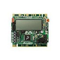
Manufacturer Part Number
TWR-S08LH64
Description
TOWER SYSTEM S08LH64
Manufacturer
Freescale Semiconductor
Type
MCUr
Datasheets
1.TWR-SENSOR-PAK.pdf
(4 pages)
2.TWR-S08LH64.pdf
(2 pages)
3.TWR-S08LH64.pdf
(19 pages)
4.TWR-S08LH64.pdf
(8 pages)
5.TWR-S08LH64.pdf
(3 pages)
Specifications of TWR-S08LH64
Contents
Board
Description/function
Tower System LCD Module
Interface Type
USB
Backlighting
No Backlighting
Data Bus Width
8 bit
Module Size (w X H X T)
3.55 in x 3.2 in
Number Of Segments
2 x 28
Operating Supply Voltage
5 V
Operating Voltage
3.3 V
Product
Display Modules
Software
Software Included
Touch Panel
No Touch Panel
Silicon Manufacturer
Freescale
Core Architecture
HCS08
Core Sub-architecture
HCS08
Silicon Core Number
MC9S08
Silicon Family Name
S08LH
Kit Contents
Board, Cable, CD
Rohs Compliant
Yes
For Use With/related Products
Freescale Tower System
Lead Free Status / RoHS Status
Lead free / RoHS Compliant


TWR-S08LH64—Lab Tutorials 1 and 2
Potentiometer vs. Light
Sensor State
This state uses two ADC channels to read
the position of the potentiometer and the
light sensed by RZ1, the on-module light
sensor. Press switch SW2 and the program
enters Potentiometer vs. Light Sensor state.
The display shows “LI” and the potentiometer
value on the large characters on the bottom
and the light sensor value on the smaller
top right two characters. The third character
displays the <, > or = char comparing the POT
to the light sensor. The two values are also
sent through the SCI port at 19.2 K baud.
1. Launch the “Serial Grapher” utility from the
2. Select your computers com port and set the
3. Click “Open Serial Port and and Start
4. The MCU is measuring the RZ1 light
Accelerometer Graphing State
Press switch SW2 and the program enters
the Accelerometer Graphing state. This
mode uses the 3-axis accelerometer, the
ADC and the SCI to measure and output the
3-axis data. Using the same setup as State
2, you will be able to graph the movement
of the accelerometer as you move the
module. Lab 2 provides a more in-depth
accelerometer demo.
Lab Tutorials for TWR-S08LH64
PEMICRO UTILITY LAUNCH PAD program.
baud rate to 19200, 8 bits, 1 stop bit, no
parity. (Typically COM1)
Demo.” Text similar to this should appear in
the terminal window:
“POT = FD Light Sensor Z1 = 56 “
“POT = FD Light Sensor Z1 = 58 “
“POT = FD Light Sensor Z1 = 65 “
sensor across a feedback resistor in an op
amp buffer with the dedicated differential
input pair DADP0 and DADM0. Adjust the
potentiometer and change the light level
reaching the light sensor and notice the
changes on the display. If ever the values
of the pot and the RZ1 are the same the
buzzer will sound and the display will show
the “=” sign.
Lab
Lab
1
1
State
State
2
3
Figure 10
ADC Demo State
Press switch SW2 again and enter the ADC
demo state. The LCD displays “ADC.” The
demo does a 16-bit conversion averaged 32
times and displays the lower 12 bits of the
16-bit result in the first three characters as
well as the channel number in the two upper
right characters. Pushing SW4 will increment
the channel converted and displayed.
This mode measures and displays the
selected ADC channel while sending the
data to the SCI output. Using the same
terminal setup as State 2 you will be able to
see the text as shown in Figure 12 being
displayed in the terminal window. Figure 11
is a short description of each of the columns
of the text output. Refer to the LH64
reference manual for detailed description of
the registers being reported.
Figure 11
Column Symbol Description
1
2
3
4
5
6
7
8
9
10
11
12
13
14
15
16
17
18
19
20
21
Lab
1
CFG1
PG
CLPD
CLPS
CLP4
CLP3
CLP2
CLP1
CLP0
MG
CLMD
CLMS
CLM4
CLM3
CLM2
CLM1
CLM0
Offset
CHNLA
DATAA
VREFT
State
Configuration Register 1
Post Calibration Plus-Side Calibration Values
Post Calibration Minus-Side Calibration Values
Calibration Offset Value
Channel for Data A
Result Data A
VERF Variable
4
Figure 12
See Figure 13 for ADC channel
assignments.
Press switch SW4 to change the channel and
watch the LCD screen and SCI output. Note
that the VREFO channel (0x13) varies since
the code is looping, modifying the trim of this
voltage reference. This demonstrates the ability
to adjust or trim the VREF output voltage.
Figure 13
Values out of RESET
CFG1= 7D
1
CFG1 PG
7D
7D
7D
7D
7D
7D
7D
7D
7D
7D
7D
7D
7D
7D
7D
ADCH
0
1
10
11
100
101
110
111
1000
1001
1010
1011
1100
10000
10001
10010
10011
10100
10101
10110
10111
11000
11001
11010
11011
11100
11101
11110
11111
2
8278 17
8278 17
8278 17
8278 17
8278 17
8278 17
8278 17
8278 17
8278 17
8278 17
8278 17
8278 17
8278 17
8278 17
8278 17
Channel
AD0
AD1
AD2
AD3
AD4
AD5
AD6
AD7
AD8
AD9
AD10
AD11
AD12
AD16
AD17
AD18
AD19
AD20
AD21
AD22
AD23
AD24
AD25
AD26
AD27
AD28
VREFH
VREFL
Module Disabled None
CFG2= 4
3
CLPD CLPS CLP4 CLP3 CLP2 CLP1 CLP0 MG
4
29
29
29
29
29
29
29
29
29
29
29
29
29
29
29
SC2= 0
5
272 013C 9F
272 013C 9F
272 013C 9F
272 013C 9F
272 013C 9F
272 013C 9F
272 013C 9F
272 013C 9F
272 013C 9F
272 013C 9F
272 013C 9F
272 013C 9F
272 013C 9F
272 013C 9F
272 013C 9F
Input
ADP0
Reserved
Reserved
Reserved
PTA0/ADP4
PTA1/ADP5
PTA2/ADP6
PTA3/ADP7
PTA4/ADP8
PTA5/ADP9
PTA6/ADP10
PTA7/ADP11
ADP12
Reserved
Reserved
Reserved
VREFO
Reserved
Reserved
Reserved
VLCD
VLL1
Reserved
Temperature Sensor N/A
Internal Bandgap
Reserved
VREFH
VREFL
6
SC3= 7
7
8
52
52
52
52
52
52
52
52
52
52
52
52
52
52
52
SC1A= 9B
9
29
29
29
29
29
29
29
29
29
29
29
29
29
29
29
Pin Control
ADPC0
ADPC1
ADPC2
ADPC3
ADPC4
ADPC5
ADPC6
ADPC7
N/A
N/A
N/A
N/A
ADPC12
N/A
N/A
N/A
N/A
N/A
N/A
N/A
N/A
N/A
N/A
N/A
N/A
N/A
N/A
N/A
10
82B4 16
82B4 16
82B4 16
82B4 16
82B4 16
82B4 16
82B4 16
82B4 16
82B4 16
82B4 16
82B4 16
82B4 16
82B4 16
82B4 16
82B4 16
SC1B= 0
11
CLMD CLMS CLM4 CLM3 CLM2 CLM1 CLM0 Offset CHNLA DATAA VREFT
12
2A
2A
2A
2A
2A
2A
2A
2A
2A
2A
2A
2A
2A
2A
2A
Below are two tables of the ADC channel
assignments as they are connected on
the Tower module. Reserved channels are
skipped in the IRQ interrupt routine to set
the next channel.
Figure 14
Figure 15
Channel (Hex)
0
1A
1B
1D
Channel (Hex)
4
5
6
7
8
9
0A
0b
0C
13
17
18
1A
1B
1D
1E
13
02BE 015A A9
02BE 015A A9
02BE 015A A9
02BE 015A A9
02BE 015A A9
02BE 015A A9
02BE 015A A9
02BE 015A A9
02BE 015A A9
02BE 015A A9
02BE 015A A9
02BE 015A A9
02BE 015A A9
02BE 015A A9
02BE 015A A9
14
15
Function 1
Potentiometer
X – Axis
Y – Axis
Z - Axis
SW3
No Connection
RZ1 Light sensor
SW2
JP10
VREFO
VLCD
VLL1
Temp Sensor
Bandgap
VREFH
VREFL
16
53
53
53
53
53
53
53
53
53
53
53
53
53
53
53
Function
Dedicated Differential Input
Temperature Sensor
Bandgap Reference
VREFH
17
2A
2A
2A
2A
2A
2A
2A
2A
2A
2A
2A
2A
2A
2A
2A
18
3
3
3
3
3
3
3
3
3
3
3
3
3
3
3
Function 2
Zero-G Accel
J2-B27
J2-B28
SW1
J1-A28
J1-A29
19
0
0
0
0
0
0
0
0
0
0
0
0
0
0
0
(sheet 2 of 2)
20
448
597
644
06D4 43
816
0D76 45
1504 46
1AAF 47
1E91
2137 49
2252
21AF
2017
1DA9
1B45
Function 3
J1-A27
21
40
41
42
44
48
4A
4B
4C
4D
4E
Accelerometer Demo
This lab will highlight the performance
capability of the MC9S08LH64
microcontroller and show how this
microcontroller can easily interface with a
sensor. It will also detail how to use one of
several software utilities included with your
TWR-S08LH64 module.
The accelerometer application reads the X,
Y and Z axes of the 3-axis accelerometer
on the TWR-S08LH64 module using the
microcontroller’s 16 bit A/D converter. It
outputs the raw values of the accelerometer
data on the microcontroller’s serial
communication interface.
Pressing the SW1 switch outputs a rolling
average of the raw accelerometer data.
Pressing the SW2 switch outputs a filtered
version. Pressing the SW3 switch reverts
back to the raw data output.
Open and Program MCU with
Accelerometer Code
1. Make sure the jumpers are in their default
2. Using CodeWarrior, click File >Open and
3. Compile the code and program the MCU by
4. When the message, “Loading a new
5. When the message, “The debugger is going
6. A debugger environment will open. From
7. Launch accelerometer utility from the
8. Set your computer’s Com port, set the baud
Lab
positions.
open the TWR9S08LH64_Accelerometer
mcp file from the directory on your c:\ where
you unzipped the compressed projects.
clicking on “Debug” button, launching the
debugger.
application will stop execution of the
current one” appears, click “OK.”
to mass erase the non-volatile memory
of the current device, then reprogram the
application” appears, click “OK.”
the main menu, choose “Run > Start/
Continue.” The program will be executed
in real-time.
PEMICRO TOOLKIT LAUNCH PAD and select
“Accelerometer.”
rate to 19200 and click “Open Serial Port
and Start Demo.”
2
Run Demo and Observe Graph
Note the X, Y and Z and C bar graphs and
the scope window on the accelerometer
graph. If the values are too small to view,
highlight a box around the graph data and
hit the play
The raw XYZ data is being displayed and
the response is very quick.
Press SW2 switch and “averaging” will be
enabled. Notice the “C” bar chart or cycle
count increase and the smoothing effect on
the XYZ data as you move the module.
Figure 16
Press SW1 switch and the FIR filter algorithm
begins executing. The cycle count will
increase again and the response of the
graph will change. Observe the change in
the graph response.
Pressing SW3 switch will return to streaming
the raw data from the accelerometer.
button in the graph window.
TOWER SYSTEM
Related parts for TWR-S08LH64
Image
Part Number
Description
Manufacturer
Datasheet
Request
R

Part Number:
Description:
Development Boards & Kits - S08 / S12 S08PT60 Tower Kit
Manufacturer:
Freescale Semiconductor
Datasheet:
Part Number:
Description:
Development Boards & Kits - S08 / S12 S08PT60Tower MCU mod
Manufacturer:
Freescale Semiconductor
Datasheet:
Part Number:
Description:
TOWER UNIVERSAL RS08/S08
Manufacturer:
Freescale Semiconductor
Datasheet:
Part Number:
Description:
K53N512CMD100 TWR Module
Manufacturer:
Freescale Semiconductor
Datasheet:
Part Number:
Description:
TWR-K53N512 Dev Kit
Manufacturer:
Freescale Semiconductor
Datasheet:

Part Number:
Description:
CONV DC/DC TRI OUT 5,15,-15V
Manufacturer:
Murata Power Solutions Inc
Datasheet:

Part Number:
Description:
CONV DC/DC TRI OUT 5,12,-12V
Manufacturer:
Murata Power Solutions Inc
Datasheet:

Part Number:
Description:
CONV DC/DC TRI OUT 5,15,-15V
Manufacturer:
Murata Power Solutions Inc
Datasheet:

Part Number:
Description:
LCD MODULE FOR TWR SYSTEM
Manufacturer:
Freescale Semiconductor
Datasheet:

Part Number:
Description:
DC/DC TH 11W 5-5/12V Triple A
Manufacturer:
Murata Power Solutions Inc
Datasheet:


Part Number:
Description:
TOWER SYSTEM PROTO
Manufacturer:
Freescale Semiconductor
Datasheet:

Part Number:
Description:
TOWER ELEVATOR BOARDS HARDWARE
Manufacturer:
Freescale Semiconductor
Datasheet: