DEMO9S08JS16 Freescale Semiconductor, DEMO9S08JS16 Datasheet - Page 19
DEMO9S08JS16
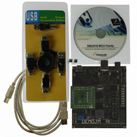
Manufacturer Part Number
DEMO9S08JS16
Description
BOARD DEMO FOR JS16 FAMILY
Manufacturer
Freescale Semiconductor
Type
MCUr
Datasheets
1.DC9S08JS16.pdf
(49 pages)
2.DEMO9S08JS16.pdf
(32 pages)
3.DEMO9S08JS16.pdf
(8 pages)
4.DEMO9S08JS16.pdf
(8 pages)
5.DEMO9S08JS16.pdf
(4 pages)
Specifications of DEMO9S08JS16
Contents
2 Boards, Cable, Documentation, DVD
Processor To Be Evaluated
MC9S08JS16
Data Bus Width
8 bit
Interface Type
USB
Operating Supply Voltage
5 V
Silicon Manufacturer
Freescale
Core Architecture
HCS08
Core Sub-architecture
HCS08
Silicon Core Number
MC9S08
Silicon Family Name
S08JS
Rohs Compliant
Yes
For Use With/related Products
MC9S08JS16
Lead Free Status / RoHS Status
Lead free / RoHS Compliant


3.9
This section describes AC timing characteristics for each peripheral system.
3.9.1
1
2
3
4
Freescale Semiconductor
3
4
5
6
7
Num
Typical values are based on characterization data at V
This is the shortest pulse that is guaranteed to be recognized as a reset pin request. Shorter pulses are not guaranteed to
override reset requests from internal sources.
This is the minimum pulse width guaranteed to pass through the pin synchronization circuitry. Shorter pulses may or may not
be recognized. In stop mode, the synchronizer is bypassed so shorter pulses can be recognized in that case.
Timing is shown with respect to 20% V
Jitter is the average deviation from the programmed frequency measured over the specified interval at maximum f
Measurements are made with the device powered by filtered supplies and clocked by a stable external clock signal. Noise
injected into the FLL circuitry via V
a given interval.
Jitter measurements are based upon a 48 MHz clock frequency.
625 ns represents 5 time quanta for CAN applications, under worst case conditions of 8 MHz CAN bus clock, 1 Mbps CAN
bus speed, and 8 time quanta per bit for bit time settings. 5 time quanta is the minimum time between a synchronization edge
and the sample point of a bit using 8 time quanta per bit.
Below D
is already in lock, then the MCG may stay in lock.
Below D
1
2
3
4
5
6
7
8
9
C
D
D
D
D
D
D
D
D
C
lock
unl
AC Characteristics
minimum, the MCG will not exit lock if already in lock. Above D
Control Timing
minimum, the MCG is guaranteed to enter lock. Above D
Bus frequency (t
Internal low-power oscillator period
External reset pulse width
(t
Reset low drive
Active background debug mode latch setup
time
Active background debug mode latch hold
time
IRQ pulse width
KBIPx pulse width
Port rise and fall time (load = 50 pF)
cyc
Asynchronous path
Synchronous path
Asynchronous path
Synchronous path
Slew rate control disabled (PTxSE = 0)
Slew rate control enabled (PTxSE = 1)
= 1/f
Self_reset
Parameter
cyc
)
= 1/f
3
3
DD
2
2
MC9S08JS16 Series MCU Data Sheet, Rev. 4
Bus
and V
DD
2
)
and 80% V
SS
Figure 13. Control Timing
and variation in crystal oscillator frequency increase the C
4
DD
DD
levels. Temperature range –40°C to 85°C.
= 5.0 V, 25 °C unless otherwise stated.
t
t
t
Symbol
ILIH,
ILIH,
Rise
t
t
t
t
MSSU
t
f
extrst
rstdrv
MSH
LPO
Bus
, t
t
t
IHIL
IHIL
Fall
lock
maximum, the MCG will not enter lock. But if the MCG
1.5 × t
unl
1.5 × t
1.5 × t
66 × t
maximum, the MCG is guaranteed to exit lock.
Min
700
100
100
DC
25
25
—
—
Self_reset
cyc
cyc
cyc
Typical
30
—
—
—
—
—
—
—
—
3
Electrical Characteristics
1
Jitter
1300
Max
24
—
—
—
—
—
—
—
—
percentage for
BUS
.
MHz
Unit
μs
ns
ns
ns
ns
ns
ns
ns
19
Related parts for DEMO9S08JS16
Image
Part Number
Description
Manufacturer
Datasheet
Request
R

Part Number:
Description:
Manufacturer:
Freescale Semiconductor, Inc
Datasheet:
Part Number:
Description:
Manufacturer:
Freescale Semiconductor, Inc
Datasheet:
Part Number:
Description:
Manufacturer:
Freescale Semiconductor, Inc
Datasheet:
Part Number:
Description:
Manufacturer:
Freescale Semiconductor, Inc
Datasheet:
Part Number:
Description:
Manufacturer:
Freescale Semiconductor, Inc
Datasheet:
Part Number:
Description:
Manufacturer:
Freescale Semiconductor, Inc
Datasheet:
Part Number:
Description:
Manufacturer:
Freescale Semiconductor, Inc
Datasheet:
Part Number:
Description:
Manufacturer:
Freescale Semiconductor, Inc
Datasheet:
Part Number:
Description:
Manufacturer:
Freescale Semiconductor, Inc
Datasheet:
Part Number:
Description:
Manufacturer:
Freescale Semiconductor, Inc
Datasheet:
Part Number:
Description:
Manufacturer:
Freescale Semiconductor, Inc
Datasheet:
Part Number:
Description:
Manufacturer:
Freescale Semiconductor, Inc
Datasheet:
Part Number:
Description:
Manufacturer:
Freescale Semiconductor, Inc
Datasheet:
Part Number:
Description:
Manufacturer:
Freescale Semiconductor, Inc
Datasheet:
Part Number:
Description:
Manufacturer:
Freescale Semiconductor, Inc
Datasheet: