C8051F912DK Silicon Laboratories Inc, C8051F912DK Datasheet - Page 17
C8051F912DK
Manufacturer Part Number
C8051F912DK
Description
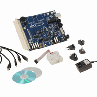
KIT DEV FOR C8051F91X/C8051F90X
Manufacturer
Silicon Laboratories Inc
Type
MCUr
Specifications of C8051F912DK
Contents
Board, Batteries, Cables, CD, Power Adapter, USB Debug Adapter
Product
Microcontroller Modules
Core Processor
C8051F9xx
Clock Speed
32.768 KHz
Interface Type
UART
Operating Supply Voltage
1.8 V to 3.6 V
Lead Free Status / RoHS Status
Contains lead / RoHS non-compliant
For Use With/related Products
C8051F91x/0x
Lead Free Status / RoHS Status
Contains lead / RoHS non-compliant
Other names
336-1854
Available stocks
Company
Part Number
Manufacturer
Quantity
Price
Company:

Part Number:
C8051F912DK
Manufacturer:
Silicon Labs
Quantity:
135


7.5. Switches and LEDs (J1, J5, J8, J15, J16)
Three push-button switches are provided on the target board. Switch SW1 (RESET) is connected to the reset pin
of the C8051F912. Pressing SW1 puts the device into its hardware-reset state. Switches SW2 (P0.2) and SW3
(P0.3) are connected to the C8051F912’s general purpose I/O (GPIO) pins through headers. Pressing SW2 or
SW3 generates a logic low signal on the port pin. Remove the shorting block from the header (J8) to disconnect the
switches from the port pins. The port pin signal is also routed to pins on the J2 and P1 I/O connectors. See Table 1
for the port pins and headers corresponding to each switch.
Two touch sensitive (contactless) switches are provided on the target board. The operation of these switches
require appropriate firmware running on the C8051F912 MCU that can sense the state of the switch. See Section
6.3. "Touch Sensitive Switch Example‚" on page 11 for details about example source code.
Five power LEDs are provided on the target board to serve as indicators. Each of the two regulators has a red LED
used to indicate the presence of power at the output of the regulator. A red USB Power LED turns on when a USB
cable is plugged into the USB connector P3. One power LED is also added to each of the two primary supply nets
powering the MCU (VDD/DC+ and VBAT). The LEDs connected to the supply nets may be disabled by removing
the shorting blocks from J1 and J5.
Two LEDs are connected to GPIO pins P1.5 and P1.6 for use by application software. See Table 1 for the port pins
and headers corresponding to each LED.
A potentiometer (R15) is also provided on the target board for generating analog signals. Place a shorting block on
J16 to connect the wiper to P0.6/CNVSTR. The header J15 allows the negative terminal of the potentiometer to be
tied to GND or to P1.4. When tied to GND, the potentiometer is always enabled and will draw a measurable
amount of supply current. When tied to P1.4, it only draws current when P1.4 is driving a logic 0 and draws no
current when P1.4 is driving a logic 1.
P1.0 (Touch Sense Switch)
P1.1 (Touch Sense Switch)
Red LED (+1 VD Power)
Red LED (+3 VD Power)
Red LED (USB Power)
Red LED (VDD/DC+)
Potentiometer (R15)
Yellow LED (P1.6)
Red LED (VBAT)
Red LED (P1.5)
Description
SW1
SW2
SW3
Table 1. Target Board I/O Descriptions
+1 VD Regulator Output
+3 VD Regulator Output
VDD/DC+ Supply Net
Rev. 0.1
VBAT Supply Net
USB VBUS
P0.6/P1.4
Reset
P0.2
P0.3
P1.0
P1.1
P1.5
P1.6
I/O
Header(s)
C8051F912-DK
J15, J16
J8[5–6]
J8[7–8]
J8[1–2]
J8[3–4]
none
none
none
none
none
none
J5
J1
17
Related parts for C8051F912DK
Image
Part Number
Description
Manufacturer
Datasheet
Request
R

Part Number:
Description:
SMD/C°/SINGLE-ENDED OUTPUT SILICON OSCILLATOR
Manufacturer:
Silicon Laboratories Inc
Part Number:
Description:
Manufacturer:
Silicon Laboratories Inc
Datasheet:
Part Number:
Description:
N/A N/A/SI4010 AES KEYFOB DEMO WITH LCD RX
Manufacturer:
Silicon Laboratories Inc
Datasheet:
Part Number:
Description:
N/A N/A/SI4010 SIMPLIFIED KEY FOB DEMO WITH LED RX
Manufacturer:
Silicon Laboratories Inc
Datasheet:
Part Number:
Description:
N/A/-40 TO 85 OC/EZLINK MODULE; F930/4432 HIGH BAND (REV E/B1)
Manufacturer:
Silicon Laboratories Inc
Part Number:
Description:
EZLink Module; F930/4432 Low Band (rev e/B1)
Manufacturer:
Silicon Laboratories Inc
Part Number:
Description:
I°/4460 10 DBM RADIO TEST CARD 434 MHZ
Manufacturer:
Silicon Laboratories Inc
Part Number:
Description:
I°/4461 14 DBM RADIO TEST CARD 868 MHZ
Manufacturer:
Silicon Laboratories Inc
Part Number:
Description:
I°/4463 20 DBM RFSWITCH RADIO TEST CARD 460 MHZ
Manufacturer:
Silicon Laboratories Inc
Part Number:
Description:
I°/4463 20 DBM RADIO TEST CARD 868 MHZ
Manufacturer:
Silicon Laboratories Inc
Part Number:
Description:
I°/4463 27 DBM RADIO TEST CARD 868 MHZ
Manufacturer:
Silicon Laboratories Inc
Part Number:
Description:
I°/4463 SKYWORKS 30 DBM RADIO TEST CARD 915 MHZ
Manufacturer:
Silicon Laboratories Inc
Part Number:
Description:
N/A N/A/-40 TO 85 OC/4463 RFMD 30 DBM RADIO TEST CARD 915 MHZ
Manufacturer:
Silicon Laboratories Inc
Part Number:
Description:
I°/4463 20 DBM RADIO TEST CARD 169 MHZ
Manufacturer:
Silicon Laboratories Inc