C8051F700DK Silicon Laboratories Inc, C8051F700DK Datasheet - Page 13
C8051F700DK
Manufacturer Part Number
C8051F700DK
Description
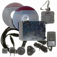
DEV KIT FOR C8051F700
Manufacturer
Silicon Laboratories Inc
Type
MCUr
Datasheets
1.C8051F700-TB.pdf
(1 pages)
2.C8051F700-TB.pdf
(306 pages)
3.C8051F700-TB.pdf
(18 pages)
Specifications of C8051F700DK
Contents
Board, Cables, CD, Debugger, Power Supply
Processor To Be Evaluated
C8051F7x
Processor Series
C8051F7xx
Interface Type
USB
Operating Supply Voltage
3.3 V
Lead Free Status / RoHS Status
Lead free / RoHS Compliant
For Use With/related Products
C8051F7xx
Lead Free Status / Rohs Status
Lead free / RoHS Compliant
Other names
336-1635


6.8. Voltage Reference (VREF) and Analog Ground Connectors (J13 and J14)
The VREF connector can be used to connect the VREF pin from the MCU (P0.0) to external 0.1 uF and 4.7 uF
decoupling capacitors. The C8051F700 device is connected to the capacitors through the J13 header. The AGND
pin from the MCU (P0.1) can be connected to the board digital ground through the J14 header.
6.9. Potentiometer (J16)
The C8051F700 device has the option to connect port pin P1.2 to a 10 k linear potentiometer. The potentiometer
is connected through the J16 header. The potentiometer can be used for testing the analog-to-digital (ADC)
converter of the MCU.
6.10. C2 Pin Sharing
On the C8051F700, the debug pin C2CK is shared with the /RST pin. The target board includes the resistor
necessary to enable pin sharing which allows the pin–shared /RST to be used normally while simultaneously
debugging the device. See Application Note “AN124: Pin Sharing Techniques for the C2 Interface” at
www.silabs.com
for more information regarding pin sharing.
Header Pins
J12[9-10]
J12[1-2]
J12[3-4]
J12[5-6]
J12[7-8]
Table 4. Serial Interface Header (J12) Description
MCU I/O Pin
none
P0.5
P0.4
P0.6
P0.7
Rev. 0.2
Board VDD to CP2103 VIO
CP2103 Pin
/RTS
/CTS
RXD
TXD
C8051F700-DK
13
Related parts for C8051F700DK
Image
Part Number
Description
Manufacturer
Datasheet
Request
R

Part Number:
Description:
SMD/C°/SINGLE-ENDED OUTPUT SILICON OSCILLATOR
Manufacturer:
Silicon Laboratories Inc
Part Number:
Description:
Manufacturer:
Silicon Laboratories Inc
Datasheet:
Part Number:
Description:
N/A N/A/SI4010 AES KEYFOB DEMO WITH LCD RX
Manufacturer:
Silicon Laboratories Inc
Datasheet:
Part Number:
Description:
N/A N/A/SI4010 SIMPLIFIED KEY FOB DEMO WITH LED RX
Manufacturer:
Silicon Laboratories Inc
Datasheet:
Part Number:
Description:
N/A/-40 TO 85 OC/EZLINK MODULE; F930/4432 HIGH BAND (REV E/B1)
Manufacturer:
Silicon Laboratories Inc
Part Number:
Description:
EZLink Module; F930/4432 Low Band (rev e/B1)
Manufacturer:
Silicon Laboratories Inc
Part Number:
Description:
I°/4460 10 DBM RADIO TEST CARD 434 MHZ
Manufacturer:
Silicon Laboratories Inc
Part Number:
Description:
I°/4461 14 DBM RADIO TEST CARD 868 MHZ
Manufacturer:
Silicon Laboratories Inc
Part Number:
Description:
I°/4463 20 DBM RFSWITCH RADIO TEST CARD 460 MHZ
Manufacturer:
Silicon Laboratories Inc
Part Number:
Description:
I°/4463 20 DBM RADIO TEST CARD 868 MHZ
Manufacturer:
Silicon Laboratories Inc
Part Number:
Description:
I°/4463 27 DBM RADIO TEST CARD 868 MHZ
Manufacturer:
Silicon Laboratories Inc
Part Number:
Description:
I°/4463 SKYWORKS 30 DBM RADIO TEST CARD 915 MHZ
Manufacturer:
Silicon Laboratories Inc
Part Number:
Description:
N/A N/A/-40 TO 85 OC/4463 RFMD 30 DBM RADIO TEST CARD 915 MHZ
Manufacturer:
Silicon Laboratories Inc
Part Number:
Description:
I°/4463 20 DBM RADIO TEST CARD 169 MHZ
Manufacturer:
Silicon Laboratories Inc