SKP38602 Renesas Electronics America, SKP38602 Datasheet - Page 13
SKP38602
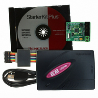
Manufacturer Part Number
SKP38602
Description
KIT STARTER FOR H8/38602
Manufacturer
Renesas Electronics America
Series
H8®r
Type
MCUr
Datasheet
1.SKP38602.pdf
(50 pages)
Specifications of SKP38602
Contents
SKP Board, In-Circuit Debugger/Programmer, Target Cable, USB Cable and SKP CD-ROM
For Use With/related Products
H8/38602
Lead Free Status / RoHS Status
Contains lead / RoHS non-compliant


■
• Max. of 85 channels can be used
• Multiple transfers or multiple types of transfers
• Supports Single, Burst, Chain and Repeat
• Data can be transferred in byte or word units
• Activation sources: interrupt and software
■
• 16bpp Direct Drive of TFT-LCD panels
• Pixel Clock, V-sync, H-sync, Data Enable
• Fully flexible for different panel sizes
• H8S/2378 drives QVGA, WQVGA panels
• H8SX/1668 drives VGA and WVGA
• CPU core is lightly loaded during LCD Direct Drive,
• Interleaved accesses allow frame buffer update for animation
■
• Two blocks of 4KB each of Data Flash
• BGO (Back Ground Operation) allows
• Erase operation can be suspended automatically to
■
• Max. of 4 channels can be used
• Dual-address or single-address
• Supports Single, Burst, Sequential,
• Data can be transferred
• Activation: internal interrupt,
mode can be selected
Idle and Repeat Transfer modes
in word or byte units
external request, auto-request
possible for one activation source
Transfer modes
and VCOM driven
and interface specifications
– WQVGA (480 x 272) driven at 116Hz
– WVGA (800 x 480) driven at 65Hz
leaving CPU core available for other system algorithms
– H8S 6% loaded, H8SX 2% loaded
available for storage of non-volatile data
Erasing or Programming of Data Flash
while executing application code.
allow Reading/Programming of User or Data Flash
DMA Controller (DMAC)
Data Transfer Controller (DTC)
TFT-LCD Direct Drive (ExDMA)
Data Flash with BGO
On-chip Peripherals: Data Transfer & Memory
H8S/2633
Single-Address Mode (Parallel read and write)
HWR, LWR
A23 to A0
DACK
RD
D15 to D0
32KB SRAM • 512KB Flash
Address bus
Peripherals
Processing
Interrupt
request
H8S CPU
Memory Map
(Virtual EEPROM)
System
Flash
(Application)
User Flash
Data Flash
H8S/2378 MCU
SRAM
Controller Chain
(Read)
Transfer Mode
(Write)
controller
Interrupt
Data Transfer
Controller
ExDMA
Flash
Data
Flash
User
Timer
(TPU)
Time
DTC
service
request
H8S/2633
Dual-Address Mode (Two-cycle read and write)
Read
HWR, LWR
BUFFER
A23 to A0
A15 to A0
Vsync, Hsync, Enable
On-chip 1KB RAM
DMA Controller Block Diagram
TFT-LCD Direct Drive (ExDMA)
Data Flash with BGO Diagram
Address Bus
EDREQ
Pixel Clock
RD
Channel n
Data Bus
n + 1
n + 2
WR/
RD/
Erase / Program
Read
D15 to D0
Address bus
Address bus
Write (2nd cycle)
Read (1st cycle)
Read
RGB
RGB
(Frame Buffer)
TFT-LCD
256K x 16
Source
Memory data
Destination
DMA Register
Source
Serial I/O
Destination
Memory
QVGA
SRAM
Read
Related parts for SKP38602
Image
Part Number
Description
Manufacturer
Datasheet
Request
R

Part Number:
Description:
KIT STARTER FOR M16C/29
Manufacturer:
Renesas Electronics America
Datasheet:

Part Number:
Description:
KIT STARTER FOR R8C/2D
Manufacturer:
Renesas Electronics America
Datasheet:

Part Number:
Description:
R0K33062P STARTER KIT
Manufacturer:
Renesas Electronics America
Datasheet:

Part Number:
Description:
KIT STARTER FOR R8C/23 E8A
Manufacturer:
Renesas Electronics America
Datasheet:

Part Number:
Description:
KIT STARTER FOR R8C/25
Manufacturer:
Renesas Electronics America
Datasheet:

Part Number:
Description:
KIT STARTER H8S2456 SHARPE DSPLY
Manufacturer:
Renesas Electronics America
Datasheet:

Part Number:
Description:
KIT STARTER FOR R8C38C
Manufacturer:
Renesas Electronics America
Datasheet:

Part Number:
Description:
KIT STARTER FOR R8C35C
Manufacturer:
Renesas Electronics America
Datasheet:

Part Number:
Description:
KIT STARTER FOR R8CL3AC+LCD APPS
Manufacturer:
Renesas Electronics America
Datasheet:
Part Number:
Description:
KIT STARTER FOR RX610
Manufacturer:
Renesas Electronics America
Datasheet:

Part Number:
Description:
KIT STARTER FOR R32C/118
Manufacturer:
Renesas Electronics America
Datasheet:

Part Number:
Description:
KIT DEV RSK-R8C/26-29
Manufacturer:
Renesas Electronics America
Datasheet:

Part Number:
Description:
KIT STARTER FOR SH7124
Manufacturer:
Renesas Electronics America
Datasheet:

Part Number:
Description:
KIT STARTER FOR H8SX/1622
Manufacturer:
Renesas Electronics America
Datasheet:

Part Number:
Description:
KIT DEV FOR SH7203
Manufacturer:
Renesas Electronics America
Datasheet: