R0K570865S000BE Renesas Electronics America, R0K570865S000BE Datasheet
R0K570865S000BE
Specifications of R0K570865S000BE


Related parts for R0K570865S000BE


R0K570865S000BE Summary of contents
Page 1
To our customers, Old Company Name in Catalogs and Other Documents st On April 1 , 2010, NEC Electronics Corporation merged with Renesas Technology Corporation, and Renesas Electronics Corporation took over all the business of both companies. Therefore, although the ...
Page 2
All information included in this document is current as of the date this document is issued. Such information, however, is subject to change without any prior notice. Before purchasing or using any Renesas Electronics products listed herein, please confirm ...
Page 3
Renesas Starter Kit for SH7086 User’s Manual RENESAS SINGLE-CHIP MICROCOMPUTER SuperH™ RISC engine Rev.1.00 2007.03 ...
Page 4
Table of Contents Chapter 1. Preface ..................................................................................................................................................1 Chapter 2. Purpose .................................................................................................................................................2 Chapter 3. Power Supply ........................................................................................................................................3 3.1. Requirements ...............................................................................................................................................3 3.2. Power – Up Behaviour .................................................................................................................................3 Chapter 4. Board Layout .........................................................................................................................................4 4.1. Component Layout .......................................................................................................................................4 4.2. Board Dimensions ........................................................................................................................................5 Chapter 5. ...
Page 5
Interrupt mask sections ............................................................................................................................27 Chapter 11. Component Placement ......................................................................................................................28 Chapter 12. Additional Information........................................................................................................................29 iii ...
Page 6
Cautions This document may be, wholly or partially, subject to change without notice. All rights reserved. No one is permitted to reproduce or duplicate, in any form, a part or this entire document without the written permission of Renesas Technology ...
Page 7
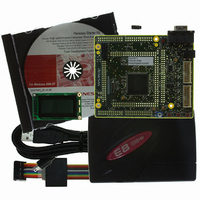
This RSK is an evaluation tool for Renesas microcontrollers. Features include: • Renesas Microcontroller Programming. • User Code Debugging. • User Circuitry such as switches, LEDs and potentiometer(s). • Sample Application. • Sample peripheral device initialisation code. The CPU board ...
Page 8
Chapter 3. Power Supply 3.1. Requirements This CPU board operates from a 5V power supply. A diode provides reverse polarity protection only if a current limiting power supply is used. All CPU boards are supplied with an E8 debugger. This ...
Page 9
Component Layout The following diagram shows top layer component layout of the board. LCD Display Microcontroller Pin Headers J3 Chapter 4. Board Layout Application Board Reset Switch Interface JA5 JA1 JA6 JA2 Potentiometer Application Board Interface ...
Page 10
Board Dimensions The following diagram gives the board dimensions and connector positions. All through hole connectors are on a common 0.1” grid for easy interfacing. Figure 4-2 : Board Dimensions 5 ...
Page 11
Chapter 5. Block Diagram Figure 5-1 shows the CPU board components and their connectivity. Figure 5-2 shows the connections to the RSK. Figure 5-1: Block Diagram Figure 5-2 : RSK Connctions 6 ...
Page 12
Switches There are four switches located on the CPU board. The function of each switch and its connection are shown in Table 6-1: Switch Functions Switch RES When pressed; the CPU board microcontroller is reset. SW1/BOOT* Connects to an ...
Page 13
Serial port The microcontroller programming serial port (SCI1) is connected to the E8 connector. This serial port can optionally be connected to the RS232 transceiver by fitting option resistors and the D connector in position 'SERIAL’. The connections to ...
Page 14
Option Links The function of the option links contained on this CPU board are listed in Table 6-5: Serial configuration links The default configuration is indicated by BOLD text Reference Function R20 Serial Port Configuration R22 Serial Port Configuration ...
Page 15
Table 6-6: Power configuration links below describes the function of the option links associated with Power configuration. The default configuration is indicated by BOLD text. Reference Function R4 Power Source R25 Power Source R26 Power R35 Power Source R36 Power ...
Page 16
The function of the option links associated with Pin function configuration are listed in Table 6-8: Pin function configuration links The default configuration is indicated by BOLD text. Reference Function R23 Pin function select R27 Pin function select R28 Pin ...
Page 17
Table 6-9: Clock configuration links below describes the function of the option links associated with Clock configuration. The default configuration is indicated by BOLD text. Reference Function R74 Clock Oscillator R75 Clock Oscillator R76 Clock Oscillator R77 Clock Oscillator 6.7. ...
Page 18
This CPU board supports four MCU operating modes and three on-chip flash memory programming modes. Jumpers can be used to set the appropriate modes while E8 is not in use. User Program mode (Mode 6) may be used to run ...
Page 19
Boot mode The boot mode settings for this CPU board are shown in Table 7-2: Boot mode pin settings FWE MD1 1 0 The following picture shows these settings made in the E8Direct configuration dialog from HEW. 7.1.2. User ...
Page 20
Chapter 8. Programming Methods All of the Flash ROM on the device can be programmed when the device is in Boot mode. In boot mode, the boot-loader program pre-programmed into the microcontroller executes and attempts a connection with the host ...
Page 21
Microcontroller Headers The microcontroller pin headers and their corresponding microcontroller connections are detailed in this section. The header pins connect directly to the microcontroller pin unless otherwise stated. * marks pins where a link to the microcontroller pin is ...
Page 22
Pin Circuit Net Name 1 DLCD5 2 DLCD6 3 DLCD7 4 VCC 5 PIN49 6 IRQ7_ADTRGn 7 ASEMD0n 8 RDn 9 WDT_OVFn 10 A18 11 A19 12 A20 13 GND 14 A21 15 A22 16 M1_TRISTn 17 PIN61 18 PIN62 ...
Page 23
Pin Circuit Net Name 1 IO_6 2 IO_5 3 IO_4 4 IO_3 5 IO_2 6 VCC 7 IO_1 8 GND 9 IO_0 10 D15 11 D14 12 D13 13 D12 14 VCC 15 D11 16 GND 17 D10 18 D9 ...
Page 24
Pin Circuit Net Name 1 TIOC0A 2 TIOC0B 3 TIOC0C 4 VCC 5 TMR0 6 RXD3 7 TXD3 8 TMR1_SCK3 9 GND 10 AVSS 11 ADPOT_AN0 12 AN1 13 AN8 14 AN9 15 AN2 16 AN3 17 AN10 18 AN11 ...
Page 25
Application Headers Standard application header connections are detailed in this section. * marks pins where a link to the microcontroller pin is via a fitted 0R link Pin Header Name CPU board Signal Name 1 5V CON_5V 2 0V(5V) ...
Page 26
Pin Header Name CPU board Signal Name 1 RESn RESn 2 EXTAL CON_EXTAL 3 NMIn NMI 4 Vss1 GROUND 5 WDT_OVF WDT_OVFn 6 SCIaTX TxD0 7 IRQ0 IRQ0 8 SCIaRX RXD0 9 IRQ1 IRQ1n 10 SCIaCK SCK0 ...
Page 27
Pin Header Name CPU board Signal Name 1 Address Bus A0 2 Address Bus A1 3 Address Bus A2 4 Address Bus A3 5 Address Bus A4 6 Address Bus A5 7 Address Bus A6 8 Address Bus A7 9 ...
Page 28
Pin Header Name CPU board Signal Name 1 AD4 AN4 2 AD5 AN5 3 AD6 AN6 4 AD7 AN7 5 CAN1TX --- 6 CAN1RX --- 7 CAN2TX --- 8 CAN2TX --- 9 Reserved 10 Reserved 11 Reserved 12 Reserved Pin ...
Page 29
Chapter 10.Code Development 10.1. Overview Note: For all code debugging using Renesas software tools, the CPU board must either be connected serial port via a serial cable USB port via an E8 ...
Page 30
HMON Components HMON is built along with the user’s code. Certain elements of the HMON code must remain at a fixed location in memory. The HMON components and their size and location in memory are detailed in Table 10-1: ...
Page 31
Memory Map The memory map shown in this section visually describes the locations of program code sections related to HMON, the FDT kernels and the supporting code within the ROM/RAM memory areas of the microcontroller. H'00000000 H'000003FF H'00000800 H'00000803 ...
Page 32
Baud Rate Setting HMON is initially set to connect at 250000 Baud. The value set in the baud rate register for the microcontroller must be altered if the user wishes to change either the serial communication baud rate of ...
Page 33
Chapter 11. Component Placement Figure 11-1: Component Placement (Top Layer) 28 ...
Page 34
Chapter 12. Additional Information For details on how to use High-performance Embedded Workshop (HEW), refer to the HEW manual available on the CD or installed in the Manual Navigator. For information about the SH7086 microcontrollers refer to the SH7080 Group ...
Page 35
Renesas Starter Kit for SH7086 User's Manual Publication Date Rev.1.00 13 March 2007 Published by: Renesas Technology Europe Ltd. Duke’s Meadow, Millboard Road, Bourne End Buckinghamshire SL8 5FH, United Kingdom ©2006 Renesas Technology Europe and Renesas Solutions Corp., All Rights ...
Page 36
Renesas Starter Kit for SH7086 1753, Shimonumabe, Nakahara-ku, Kawasaki-shi, Kanagawa 211-8668 Japan User’s Manual REG10J0028-0100 ...