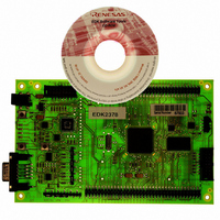
EDK2378 Renesas Electronics America, EDK2378 Datasheet
EDK2378
Specifications of EDK2378


Related parts for EDK2378


EDK2378 Summary of contents
Page 1
... EDK2378 U M SER ANUAL F H8S/2378 FLASH M N CHIP ICROCONTROLLER ...
Page 2
Preface Cautions 1. This document may be, wholly or partially, subject to change without notice. 2. All rights reserved. No one is permitted to reproduce or duplicate, in any form, a part or this entire document without Renesas Technology Europe ...
Page 3
T C ABLE OF ONTENTS ............................................................................................................................................. 3 ABLE OF ONTENTS ....................................................................................................................................... 4 TART UP NSTRUCTIONS 2.1. INSTALLING THE EVALUATION DEVELOPMENT KIT (EDK)........................................................................... 4 2.2. SERIAL CONNECTION ....................................................................................................................................... 4 2.3. POWER SUPPLY ................................................................................................................................................ ...
Page 4
TART UP NSTRUCTIONS 2. NSTALLING THE VALUATION Please refer to the quick start guide provided for initial installation of the EDK. A copy of the quick start guide and other information relating to this ...
Page 5
EDK B L OARD AYOUT The diagram shows a general layout of the EDK board. FLASH Programming Power NMI Switch BOOT LED Power LED User1 LED User2 LED RESET BOOT Switch Switch CJ5 9-Way D-Type CJ4 3.1. EDK B ...
Page 6
EDK O PERATION 4.1. USER INTERFACE The EDK provides three buttons for influencing the operation of the board. The purpose of each button is clearly marked next to it. Refer to the board layout for positions (Section 3) 1. ...
Page 7
C C RYSTAL HOICE The operating crystal frequency has been chosen to support the fastest operation with the fastest serial operating speeds. The value of the crystal is 14.7456MHz. The HMON tutorial code configures the PLL control register (PLLCR) ...
Page 8
M M EMORY AP Table 4-4 illustrates the EDK memory map for mode 4. Section End Section Start H’000000 H’07FFFF H’080000 H’0BFFFF H’0A0000 H’1FFFFF H’200000 H’FF3FFF H’FF4000 H’FFBFFF H’FFC000 H’FFCFFF H’FFD000 H’FFFBFF H’FFFC00 H’FFFEFF H’FFFF00 H’FFFF1F H’FFFF20 H’FFFFFF 4.5. ...
Page 9
B O OARD PTIONS The EDK has a number of configuration settings set by jumpers CJ4 ( CJ5 ( and zero-ohm links. Common EDK functions can be set using the jumpers as described ...
Page 10
– CJ5 SER ODE ETTINGS CJ5 is used to set the operating mode of the microcontroller. These jumpers must be fitted at all times to ensure correct operation of the EDK. Jumper CJ 5-A User Mode ...
Page 11
ERIAL ORT ELECTION The programming serial port is connected to the RS232 connector by default. This allows direct programming of the EDK using the supplied software tools. A secondary serial port is available on the microcontroller ...
Page 12
EXTERNAL DEBUG HEADER The External debug header may be used with the Renesas E10A Debugger or a third party debugger. The E10A is an on-chip debug emulator available separately from Renesas. This header provides direct access for the debugger ...
Page 13
S D TATE IAGRAM Async Boot Mode Controller : Positive Logic (CTS+BootSw) . /Res Waiting Reset Timer /Res ResSw . /Res Res /Res . Reset Reset (BootSW + ResSw + CTS) . /Res F 5-2: CPLD S D IGURE ...
Page 14
M ICROCONTROLLER The following table lists the connections to each or the headers on the board. 6. EADER Pin Function No 1 Vss 3 PLLVss 5 PLLVcc 7 PF5/RDn 9 PF3/LWRn 11 PF1/IRQ14n/UCASn/DQMU 13 P62/TEND0n/TMCIO/IRQ10n 15 P60/DREQ0n/TMRIO/IRQ8n ...
Page 15
H J2 EADER Pin Function No 1 XTAL 3 Vcc Vss 9 P63/TEND1n/TMCI1/IRQ11n 11 P65/DACK1n/TMO1/IRQ13n 13 PG1/CS1n 15 PG3/CS3n/RAS3n/CASn 17 Vref 19 P41/AN1 21 P43/AN3 23 P45/AN5 25 P47/AN7/DA1 27 P91/AN9 29 P93/AN11 31 P95/AN13/DA3 33 ...
Page 16
C D ODE EVELOPMENT 7.1. HMON 7.1. ODE UPPORT The HMON library is built to support Advanced Expanded Mode only. The Device supports only Mode 4. 7.1. REAKPOINT UPPORT The monitor has no PC Break ...
Page 17
M M EMORY AP H'00000000 Vectors H'00001000 FDTUserModeMicr oKernel H'00001119 H'00002000 CUser_Vectors H'00002003 H'00005000 PHMON CHMON H'00007441 On-Chip FLASH ROM H'0007FFFF H'00FFB000 On-Chip RAM H'00FF4432 BHMON H'00FF4640 H'00FFA000 Stack H'00FFA1FF H'00FFBFFF H'00FFFC00 Internal I/O REGISTERS H'00FFFF00 H'00FFFF20 Internal I/O ...
Page 18
AUD ATE ETTING HMON has initially set to connect at 115200Baud. Should the user wish to change this, the value for the BRR in HMONserialconfiguser.c will need to be changed and the project re-built. Please refer ...